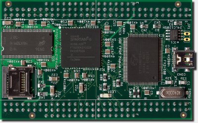
USB-FPGA Module 1.11:
Spartan 6 LX9 to LX25 FPGA Board with USB 2.0 Microcontroller and 64 MByte DDR SDRAM
USB-FPGA Modules 1.11 are deprecated. Please switch to Series 2 FPGA Boards.
An Adapter is available as workaround.
The old product page is still available here for documentation purposes.
|
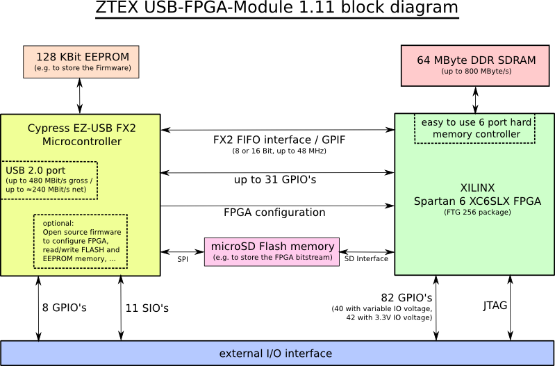
Block diagram
Schematics (PDF) |
 |
Block diagram
Features
- High-Speed (480 MBit/s) USB interface via Mini-USB connector (B-type)
- Cypress CY7C68013A EZ-USB FX2 Microcontroller
- Xilinx Spartan 6 LX9 to LX25 FPGA (XC6SLX9 to XC6SLX25), see Variants
-
90 General Purpose I/O's (GPIO):
- 82 FPGA GPIO's
- 8 EZ-USB FX2 GPIO's
-
15 special I/O's (SIO):
- 4 pins for FPGA configuration via JTAG
- 2 pins for 1 serial ports
- 2 pins I2C interface (2 pins)
- 2 interrupt pins
- 3 timers
- 1 Wakeup pin
- 1 Breakpoint pin
-
64 MByte DDR SDRAM:
- 200 MHz clock frequency
- 16 Bit bus width
- Up to 800 MByte/s data rate
- Easy to use hard memory controller included Spartan 6 FPGA with 6 ports. (see SDK for examples)
- MicroSD socket for extensible Flash memory (standard and high capacity (SDHC) cards, SPI mode support required)
- 128 Kbit EEPROM memory (can be used to store the EZ-USB firmware)
- External power supply required:
- 3.3 V; supply current depends on application (see Spartan 6 datasheets), recommended: ≥ 500 mA
- 2.5 V - 2.6 V; supply current depends on application (see Spartan 6 datasheets), recommended: ≥ 900 mA
- 1.2 V; supply current depends on application (see Spartan 6 datasheets), recommended: XC6SLX9: ≥ 500 mA, XC6SLX16: ≥ 750mA, XC6SLX25: ≥ 1000 mA
- Variable I/O voltage VCCO_IO: 1.14...3.46 V; supply current depends on application (see Spartan 6 datasheets), recommended: ≥ 500 mA
- Temperature range: 0-70°C (-25°C - 85°C on request)
- FPGA configuration / programming via USB using the EZ-USB FX2 SDK. (No JTAG adapters or other additional utilities required.)
- FPGA configuration / programming from Flash memory
Variants
Variants with different features are offered:
| Variant | FPGA | Speed grade (larger means faster) |
Female pin headers on bottom side (two 2x32 und two 1x16) |
Availability |
| USB-FPGA Module 1.11a | XC6SLX9 | 2 | Yes | Out of stock, please switch to Series 2 FPGA Boards |
| USB-FPGA Module 1.11b | XC6SLX16 | 2 | No | |
| USB-FPGA Module 1.11c | XC6SLX25 | 3 | Yes |
Other variants (with or without pin headers, other speed grades, extended temperature range) can be produced on request.
SDK, Examples, Getting Started
A powerful open source Firmware Development Kit with platform independent host software API is available for the FPGA Board. This SDK allows to define all USB device descriptors using only a few macro commands, and thus gives the developer a quick start into Firmware programming.The SDK package contains a lot of examples which can be used as starting point for own applications.
More Information are available in the EZ-USB FX2 SDK section.
Additional documentation including Tutorials can also be found on the ZTEX Wiki
Functional description
The following drawing shows the measurements and the location of the of the described elements.
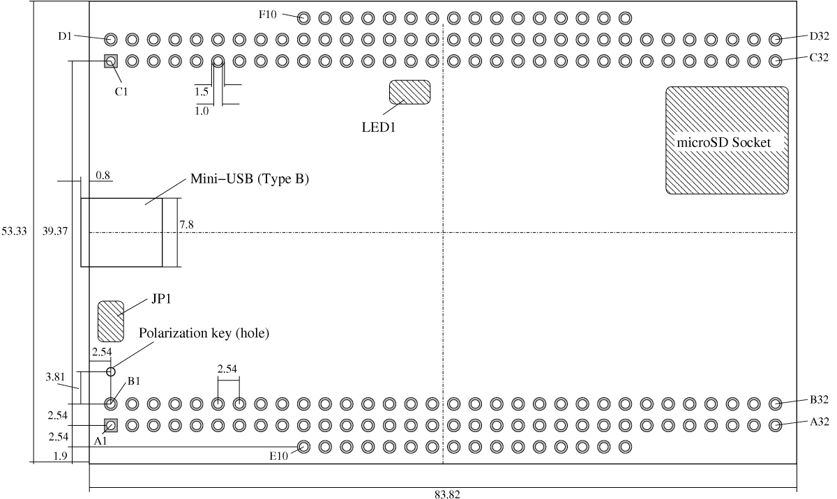
Click on the image for a larger version or download the PDF version.
FPGA configuration
There are three ways to configure the FPGA:- From USB with the SDK. This can be done using the API (see configureFpga) or using the utilities FWLoader or DeviceServer. DeviceServer allows comfortable access to the FPGA Board using the http interface and your Web browser as GUI.
- Via JTAG, see JTAG section below. Bitstream upload via JTAG is slow. Therefore the USB method should be preferred.
- From microSD, see the standalone description on the ZTEX Wiki.
EEPROM address: JP1
Jumper JP1 specifies the I2C address of the EEPROM:
| JP1 | I2C address |
| open | 0xA2 |
| close | 0xAA |
The EZ-USB FX2 Microcontroller searches for the firmware at the address 0xA2 which is the default address (jumper open).
The main purpose of this jumper is to disable EEPROM boot-loading. If, for example, the EEPROM was programmed with a corrupt firmware the Microcontroller can be booted with the internal firmware by closing JP1 during powering-on the FPGA Board.
FPGA state: LED1
LED1 indicates the configuration state of the FPGA as follows:
| LED1 | FPGA |
| on | unconfigured |
| off | configured |
Clock resources
On the FPGA board two clocks sources are connected to the FPGA: the clock output of the EZ-USB FX2 which is usually configured to 48 MHz and the interface clock which can be configured to 30 MHz or to 48 MHz. They can be used to generate new clocks within the FPGA using DCM's or PLL's.Additional clocks can be connect to the GCLK pins of the I/O connector.
In most cases the on board clock sources are sufficient.
I/O Connector
Two 2x32 pin and two 1x16 pin connectors deliver the I/O signals and are used for the power supply. The drawing shows the position of these connectors.
The I/O connector of the Spartan 6 USB-FPGA Module 1.11 is mechanical downward compatible to the I/O Connector of the USB-FPGA Module 1.2.
There is a polarization key in form of a small hole close to the B1 pin as shown on the drawing. In order to prevent damage equal orientation of the polarization key (hole) of all stacked boards must be ensured.
JTAG
The FPGA can be configured either via USB or via JTAG. JTAG signals are available at Pins D29 to D32 of the I/O connector. On the Experimental Board and the Power Supply Module JTAG signals are provided at a 8 or 14 pin header.
If the JTAG interface is used for FPGA configuration bit 1 of port A (=PROG_B at FPGA) must be driven high. This happens automatically if a firmware developed with the SDK is running.
Pinlist and List of Connections
The Pinlist of the I/O Connector and the List of Connections can be downloaded in Gnumeric or Excel format. These files contain the data for all USB-FPGA Boards including compatibility information. (Attention: The files contain several sheets.)
This is the Pinlist of the I/O Connector:
Pinlist
E
A
B
C
D
F
1
4..35V
4..35V
USB_5V
USB_5V
1
2
GND
GND
5V (unused)
5V (unused)
2
3
INT4
T0
R16~IO_L49N_M1DQ11_1
5V (unused)
3
4
T1
T2
GND
GND
4
5
BKPT
GND
INT5#
WAKEUP*
5
6
SCL
SDA
3.3V
3.3V
6
7
3.3V
3.3V
7
8
TxD0
RxD0
GND
K16~IO_L44N_A2_M1DQ7_1
8
9
B15~IO_L29P_A23_M1A13_1
B16~IO_L29N_A22_M1A14_1
PE7/GPIFADR8
L16~IO_L47N_LDC_M1DQ1_1
9
10
2.5V
2.5V
PE6/T2EX
M16~IO_L46N_FOE_B_M1DQ3_1
N16~IO_L45N_A0_M1LDQSN_1
10
11
1.2V
1.2V
PE5/INT6
P16~IO_L48N_M1DQ9_1
M15~IO_L46P_FCS_B_M1DQ2_1
11
12
A14~IO_L65N_SCP2_0
B14~IO_L65P_SCP3_0
PE4/RXD1OUT
P15~IO_L48P_HDC_M1DQ8_1
R15~IO_L49P_M1DQ10_1
12
13
A13~IO_L63N_SCP6_0
C13~IO_L63P_SCP7_0
GND
PE3/RXD0OUT
T15~IO_L50N_M1UDQSN_1
L14~IO_L47P_FWE_B_M1DQ0_1
13
14
C11~IO_L39P_0
D12~IO_L66N_SCP0_0
D11~IO_L66P_SCP1_0
PE2/T2OUT
K15~IO_L44P_A3_M1DQ6_1
N14~IO_L45P_A1_M1LDQS_1
14
15
A11~IO_L39N_0
E11~IO_L64N_SCP4_0
F10~IO_L64P_SCP5_0
PE1/T1OUT
R14~IO_L50P_M1UDQS_1
L13~IO_L53N_VREF_1
15
16
B10~IO_L35P_GCLK17_0
3.3V
3.3V
PE0/T0OUT
M13~IO_L74P_AWAKE_1
L12~IO_L53P_1
16
17
A10~IO_L35N_GCLK16_0
C10~IO_L37N_GCLK12_0
E10~IO_L37P_GCLK13_0
GND
M12~IO_L2P_CMPCLK_2
R12~IO_L52P_M1DQ14_1
17
18
F9~IO_L40P_0
B12~IO_L62P_0
A12~IO_L62N_VREF_0
2.5V
2.5V
M11~IO_L2N_CMPMOSI_2
18
19
D9~IO_L40N_0
A9~IO_L34N_GCLK18_0
C9~IO_L34P_GCLK19_0
1.2V
T12~IO_L52N_M1DQ15_1
M10~IO_L16N_VREF_2
19
20
A8~IO_L33N_0
C8~IO_L38N_VREF_0
D8~IO_L38P_0
P8~IO_L30P_GCLK1_D13_2
R9~IO_L23P_2
T9~IO_L23N_2
20
21
B8~IO_L33P_0
GND
GND
M9~IO_L29P_GCLK3_2
N9~IO_L14P_D11_2
P9~IO_L14N_D12_2
21
22
E8~IO_L36N_GCLK14_0
VCCO_IO
VCCO_IO
T7~IO_L32N_GCLK28_2
N8~IO_L29N_GCLK2_2
T8~IO_L30N_GCLK0_USERCCLK_2
22
23
E7~IO_L36P_GCLK15_0
1.2V
1.2V
M7~IO_L31N_GCLK30_D15_2
P7~IO_L31P_GCLK31_D14_2
R7~IO_L32P_GCLK29_2
23
24
A7~IO_L6N_0
C7~IO_L6P_0
N6~IO_L64N_D9_2
P6~IO_L47P_2
T6~IO_L47N_2
24
25
E6~IO_L5N_0
F7~IO_L5P_0
M6~IO_L64P_D8_2
P4~IO_L63P_2
T4~IO_L63N_2
25
26
C6~IO_L7N_0
D6~IO_L7P_0
GND
GND
26
27
A6~IO_L4N_0
B6~IO_L4P_0
27
28
C5~IO_L3N_0
D5~IO_L3P_0
1.2V
1.2V
28
29
A5~IO_L2N_0
B5~IO_L2P_0
2.5V
TDI
29
30
A4~IO_L1N_VREF_0
C4~IO_L1P_HSWAPEN_0
TMS
30
31
VCCO_IO
VCCO_IO
TCK
31
32
GND
GND
GND
TDO
32
| Summary | ||||
| A/B/E | C/D/F | |||
| FPGA-IO | 42 | FPGA-IO | 40 | |
| Serial | 2 | FX2-IO | 8 | |
| I2C | 2 | Wakeup | 1 | |
| Timer | 3 | JTAG | 4 | |
| Interrupt | 1 | Interrupt | 1 | |
| Breakpoint | 1 | USB 5V | 2 | |
| GND | 8 | GND | 7 | |
| 3.3V | 4 | 3.3V | 2 | |
| 1.2V | 4 | 1.2V | 3 | |
| 2.5V | 2 | 2.5V | 3 | |
| VCCO_IO | 4 | 5V | 3 | |
| 4..35V | 2 | NC | 6 | |
| NC | 5 | |||
| FPGA-GPIO | 42 | FPGA-GPIO | 40 | |
| SIO (special I/O) | 9 | FX2-GPIO | 8 | |
| Power | 24 | SIO (special I/O) | 6 | |
| NC | 5 | Power | 20 | |
| Sum | 80 | NC | 6 | |
| Sum | 80 | |||
Images
Click on the images for larger versions.
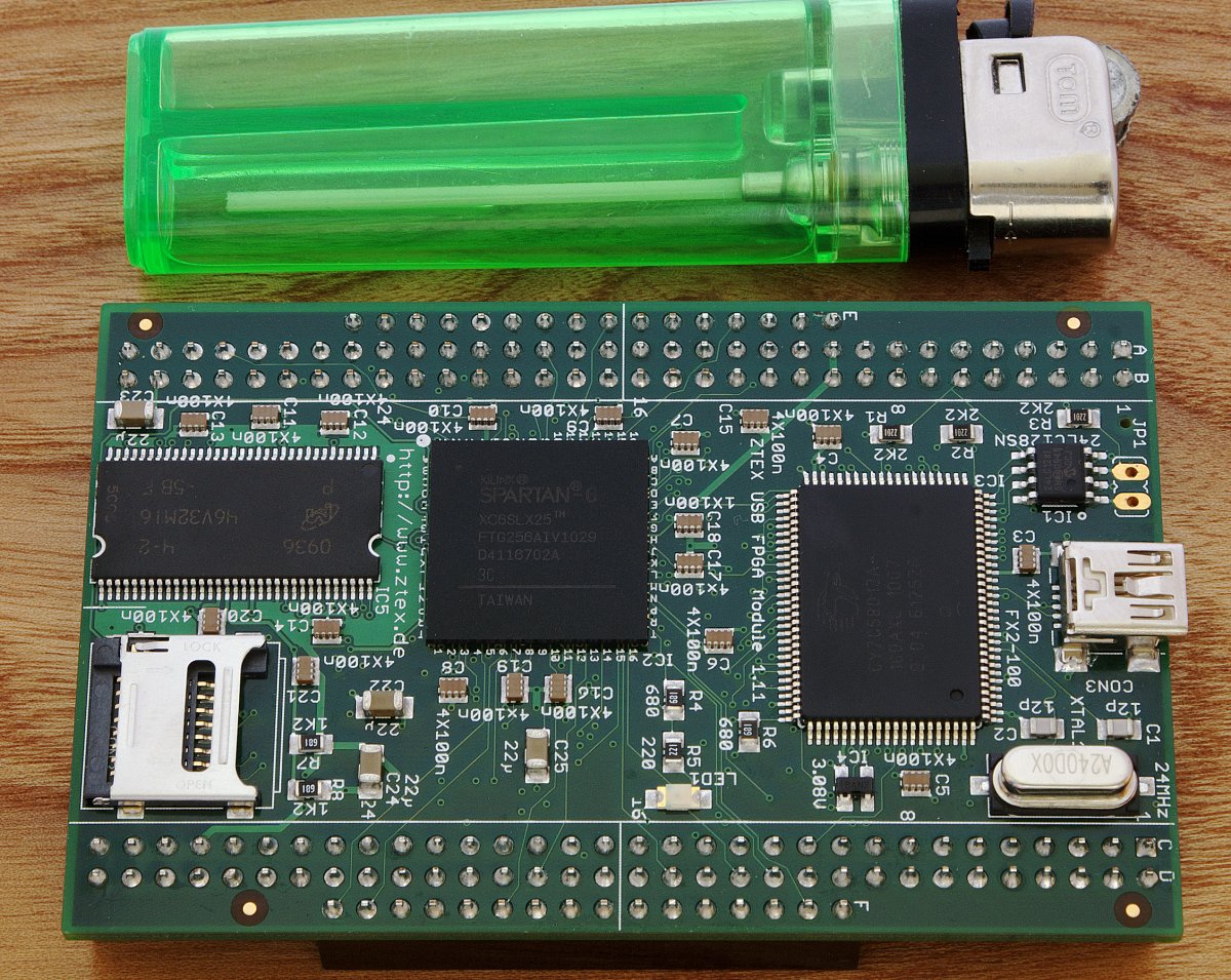
Size comparison of the Spartan 6 USB-FPGA Module 1.11c with installed female pin headers on the bottom side. |
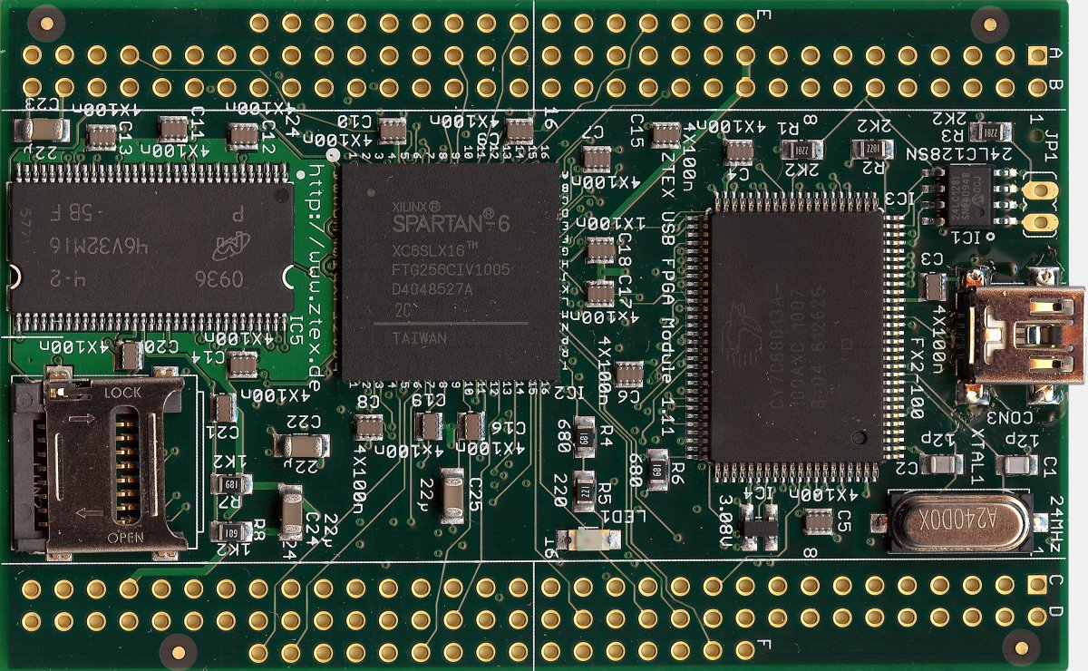
Top side of the Spartan 6 USB-FPGA Module 1.11b. |