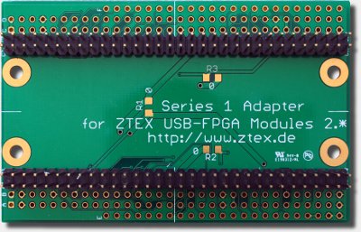
Series 1 Adapter for Series 2 FPGA Boards
|
The Series 1 Adapter board allows to use Series 2 FPGA Boards on application circuits for USB-FPGA Modules 1.∗. It also can be used as mounting adapter if no application circuit is present. Usage instructionThe Series 1 Adapter can replace USB-FPGA Modules 1.∗ alone or in combination with a Power Supply Module. Depending on the usage, some of the 0 Ω resistors R1, R2 or R3 (package 1206; a piece of wire can be used instead) may be installed (also see the schematics). In order to prevent damage a few rules have to be kept:
Additional resources
Schematics (PDF) |
 |
Pin assignment and net list
The pin assignment and net list can also be downloaded in Gnumeric or Excel format (several sheets).
The table shows the pin assignment of the Series 1 connector, e.g. pin A20 if the Series 1 connector is connected to pin A19 of the Series 2 FPGA Board.
Pin assignment
E
A
B
C
D
F
1
VIN
VIN
USB_5V
USB_5V
1
2
GND
GND
2
3
C3
3
4
GND
GND
4
5
BKPT
GND
5
6
A3
B3
3.3V
3.3V
6
7
3.3V
3.3V
VCCO_CD
VCCO_CD
7
8
A4
B4
GND
D3
8
9
A5
B5
C4
D4
9
10
C5
D5
C6
10
11
D6
C7
D7
11
12
A6
B6
C8
D8
C9
12
13
B7
A7
GND
D9
C10
D10
13
14
A9
A8
B8
C11
D11
C12
14
15
B10
B9
A10
D12
C13
D13
15
16
A11
3.3V
3.3V
C14
D14
C15
16
17
B12
B11
A12
GND
D15
C19
17
18
A14
A13
B13
D19
18
19
B18
B14
A18
C20
D20
19
20
A20
A19
B19
C21
D21
C22
20
21
B20
GND
GND
D22
C23
D23
21
22
A21
VCCO_AB
VCCO_AB
C24
D24
C25
22
23
B21
D25
C26
D26
23
24
A23
A22
B22
C27
D27
C28
24
25
B24
B23
A24
D28
C29
D29
25
26
A26
A25
B25
GND
GND
26
27
B27
B26
A27
VCCO_CD
VCCO_CD
C30
27
28
A28
B28
D30
28
29
3.3V
A29
B29
29
30
3.3V
A30
B30
30
31
GND
VCCO_AB
VCCO_IO
31
32
GND
GND
GND
GND
Variants
Two variants are available in the shop:
| Series 2 pin headers | Series 1 pin headers | Shop link |
| Male pin headers on top side | not installed | to the Shop |
| Male pin headers on top side | Two 2x32 and two 1x23 female pin headers on | to the Shop |
Images

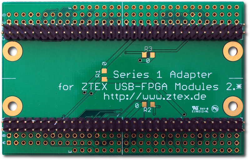
Top side of Series 1 Adapter for ZTEX Series 2 FPGA Boards (variant without female pin headers). |

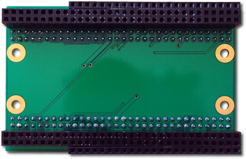
Bottom side of Series 1 Adapter for ZTEX Series 2 FPGA Boards (variant with female pin headers). |