USB-FPGA Module 2.18:
Artix 7 XC7A200T FPGA Board with EZ-USB FX3S and DDR3 SDRAM.
|
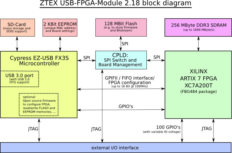
Block diagram |
 |
Schematics (PDF)
Source files and jed file for Board Management CPLD
Pin assignment and net list (Gnumeric format, several sheets)
Pin assignment and net list (Excel format, several sheets)
Eagle Library of the I/O connector
I/O trace length
![]() Xilinx Artix 7 Family datasheets from the Xilinx homepage
Xilinx Artix 7 Family datasheets from the Xilinx homepage
![]() CYUSB3033: EZ-USB FX3S datasheet from the Cypress homepage
CYUSB3033: EZ-USB FX3S datasheet from the Cypress homepage
![]() EZ-USB FX3 Technical Reference Manual from the Cypress homepage
EZ-USB FX3 Technical Reference Manual from the Cypress homepage
Debug Board
Series 1 Adapter Board
Cluster base board
Block diagram
Features
- Xilinx Artix 7 FPGA XC7A200T
- USB 3.0 interface with Micro-USB connector
- Cypress CYUSB3033 EZ-USB FX3S Microcontroller:
- ARM926EJ core at 208 MHz
- 512 KByte SRAM
- 1 Storage Port
- 16 Bit GPIF II at 104 MHz (bandwidth between EZ-USB FX3S and FPGA: 208 MByte/s)
- USB 2.0 OTG host support (FPGA board acts as host)
- External I/O connector (consisting in two female 2x32 pin headers with 2.54mm grid) provides:
- 100 General Purpose I/O's (GPIO) connected to FPGA
- JTAG signals
- Reset signal
- External power (5 V .. 16 V) input
- 3.3V output
- I/O voltage output or input, see External I/O connector
-
256 MByte DDR3 SDRAM:
- Up to 400 MHz clock frequency
- 16 Bit bus width
- Up to 1600 MByte/s data rate
- Usable with the Xilinx Memory Interface Generator (MIG), examples are included in the SDK
- 128 MBit on-board Flash memory
- Firmware storage and auto-boot
- Bitstream storage and auto-boot
- Accessible from EZ-USB FX3S and from FPGA, see the CPLD description
- SD card socket
- SD 3.0 (SDXC) support
- SDIO 3.0 support
- 2 Kbit MAC-EEPROM: contains a unique non erasable MAC-address and is used to store firmware settings
- On-Board power supply:
- External power (5 V .. 16 V)
- 5.0 V: 400 mA
- 3.3 V: 3000 mA
- 1.8 V: 1500 mA
- 1.5 V: 1500 mA
- 1.2 V: 1500 mA
- 1.0 V: 14000 mA
- OTG supply switchable and reverse current protected
- Heat sink for high performance / high speed applications, see Section heat sink
- Optional:
- Battery to store a key for bitstream encryption
- Free of charge development software: Vivado Webpack for FPGA and ZTEX SDK for firmware and host software.
- Temperature range: Board: 0-70°C; max. FPGA temperature see below
Variants
Only one variant of this FPGA Board is available:
| Variant | FPGA | Speed grade (larger means faster) |
FPGA temperature | Availability |
| USB-FPGA Module 2.18b | XC7A200T | 2C | 0-85°C | Replaced by faster and fully compatible variant 2.18b2. Remainders in the Shop |
| USB-FPGA Module 2.18b2 | XC7A200T | 3E | 0-100°C | Stock type, to the Shop |
Functional description
The following drawing shows the measurements and the location of the described elements.
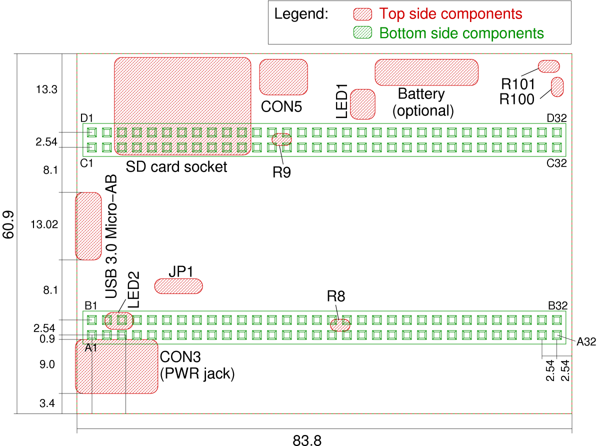
Click on the image for a larger version or download the PDF version.
The USB-FPGA Module 2.18 is usually plugged onto an application circuit and therefore has no mounting holes. If a mounting adapter is needed, one of the add-on cards can be used for this purpose.
Common functions of all Series 2 FPGA Boards
The USB-FPGA Module 2.18 is a member of ZTEX FPGA Board Series 2. All functions that are shared with the other boards of this Series are described on the Series 2 FPGA Board pageJP1
Jumper JP1 is used to disable booting from Flash during, see Firmware loading. JP1 has an unconnected pin which can be used for parking the jumper. The following pictures show all possible jumper positions:
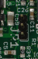
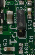
|
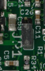
|
| JP1 open | JP1 closed |
Internals about the mechanism of disabling Flash can be found in the CPLD description.
LED1, LED2
LED1 is a duo-LED which is connected to the FPGA. The single LED2 is connected to the EZ-USB FX3. Functions are listed in the following table:| LED1, short wavelength | FPGA configuration state: on if unconfigured |
| LED1, long wavelength | User defined: connected to FPGA pin T11, output is inverted |
| LED2 |
User defined: connected to GPIO53 of EZ-USB FX3 (Firmware: ZTEX_GPIO_LED) Default Firmware: on if USB is connected |
Powering, CON3
The USB-FPGA Module 2.18 must be powered by an external supply via CON3 or pins A1 and B1 of the external I/O connector. CON3 is a standard DC power jack with 2.1mm center pin (+) diameter and 5.5mm barrel (-) diameter. A1 and B1 of the I/O connector and the center pin of CON3 are connected directly. This allows to supply a base board from the FPGA board.Valid supply voltage is 5 V to 16 V. If a fan is installed to CON5, the input voltage should be about 12V.
SD card
The USB-FPGA Module 2.18 have a SD card socket which is connected to S-Port 0 of the FX3. The SDK supports SD cards as secondary Flash device. The implementation of this feature should be considered as a demo. In order to make use from the full feature set (SDIO, higher speeds, file system support) the Cypress SDK has to be used.External I/O Connector
The external I/O connector is compatible to other FPGA Boards of the Series 2 and therefore described at page of Series 2 FPGA Boards.On the USB-FPGA Module 2.18 all 100 external I/O's are assigned and have a variable I/O voltage. I/O voltage for rows A and B is VCCO_AB and for rows C and D it is VCCO_CD. By default VCCO_AB and VCCO_CD are connected to 3.3V through 0Ω resistors R8 and R9, respectively. Thus, these pins are 3.3V outputs. (This is the standard behaviour for all FPGA Boards of the Series 2.) If another I/O voltage is required, R8 and/or R9 can be unsoldered and VCCO_AB and/or VCCO_CD can be used as voltage input.
Clock resources
On the FPGA Board two clocks sources are connected to the FPGA, a 26 MHz signal and the interface clock which can be configured. If default firmware is used, frequency of the interface clock is 104 MHz.Additional clocks can be connect to the MRCC and SRCC pins of the I/O connector. (These pins are arranged as differential pairs, e.g. L12P_T1_MRCC_35 and L12N_T1_MRCC_35. Single ended clocks must be connected to the positive pin, e.g. L12P_T1_MRCC_35.)
In most cases the on board clock sources are sufficient. It's recommended to derive internal clocks from the fixed 26 MHz clock.
Board Management CPLD
The CPLD provides several board management functions:- FX3 reset controller: delayed deassertion of reset signal
- FPGA reset controller: asserted by FX3 or by global reset signal
- SPI Switch: see below
- Flash disabling: using JP1 or by FX3, see below
- Clock signal duplication (in order to assure signal quality)
- Disabling Flash
- Soft reset EZ-USB FX3
- EZ-USB FX3 restarts with internal firmware and waits for being reprogrammed via USB
- Writing new Firmware to FX3 via USB and starting the firmware
| Input | Output | |||
| M0:M1 | JP1 | Current state | Next state | SPI: Master → Slave |
| 0:0 | * | * | S1 | FX3 → FPGA |
| 1:0 | * | * | S2 | FPGA → Flash |
| *:1 | open | start,S3,S4 | S3 | FX3 → Flash |
| *:1 | closed | start,S3,S4 | S4 | disabled |
| *:1 | * | S1,S5 | S5 | FX3 → Flash |
| *:1 | * | S2,S6 | S6 | disabled |
CPLD is controlled by the firmware, i.e. users not need to take care about the CPLD internals mentioned above.
Source files can be found in CPLD package. The CPLD is factory programmed.
USB OTG
The EZ-USB FX3 supports USB-2.0 OTG, i.e. the FPGA Board can act as USB-2.0 host. In OTG mode the 5V USB supply must be driven by the FPGA Board. This function is controlled by GPIO57 of FX3 or using the functions ztex_enable_otg_supply()/ztex_disable_otg_supply() of the firmware kit.Heat sink, CON5
For high performance / high speed applications a heat sink is required. On USB-FPGA Module 2.18 standard heat sinks with two push-pins and a distance of 59mm can be installed.CON5 is a standard 3 pin fan connector for active coolers. If this connector is used the input voltage should be between 9V and 13V.
The USB-FPGA Module 2.18 is delivered with a cooling kit consisting in:
- 1 passive heat sink; height: 13mmm
- 1 active cooler; height with fan: 24mm
- 2 thermal pads with low thermal resistance
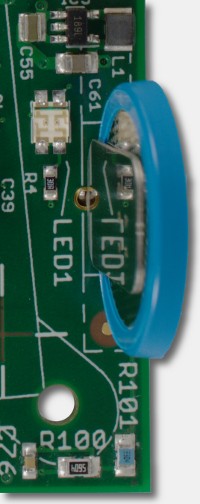
JTAGThe FPGA can be configured either via USB or via JTAG. JTAG signals are available on the external I/O connector and JTAG headers are installed on most add-on cards.The JTAG interface can also be used for re-programming the CPLD. Battery optionIf Bitstream encryption is required a standard 3V Lithium battery with a pin distance of 10×3mm can be installed. Furthermore two 0805 SMD resistors need to be soldered, R100: 5.6 MΩ and R101: 3.3 MΩ. Taking into account the battery degeneration the data retention time should be at least 10 years.The battery allows the FPGA to store a key which is used for bitstream encryption in a special low-power memory. The key has to be uploaded via JTAG. In order to prevent damage R100 must be soldered before the battery is installed. Also care should be taken in order to prevent shortcuts at the battery that can cause voltage drop and loss of encryption data. The picture on the right shows an USB-FPGA Module 2.18 with installed battery, R100 and R101. FPGA Boards with factory-installed battery components are available on request. Instructions for Bitstream encryption can be found on the Wiki. |
 |
Images
Click on the images for larger versions.
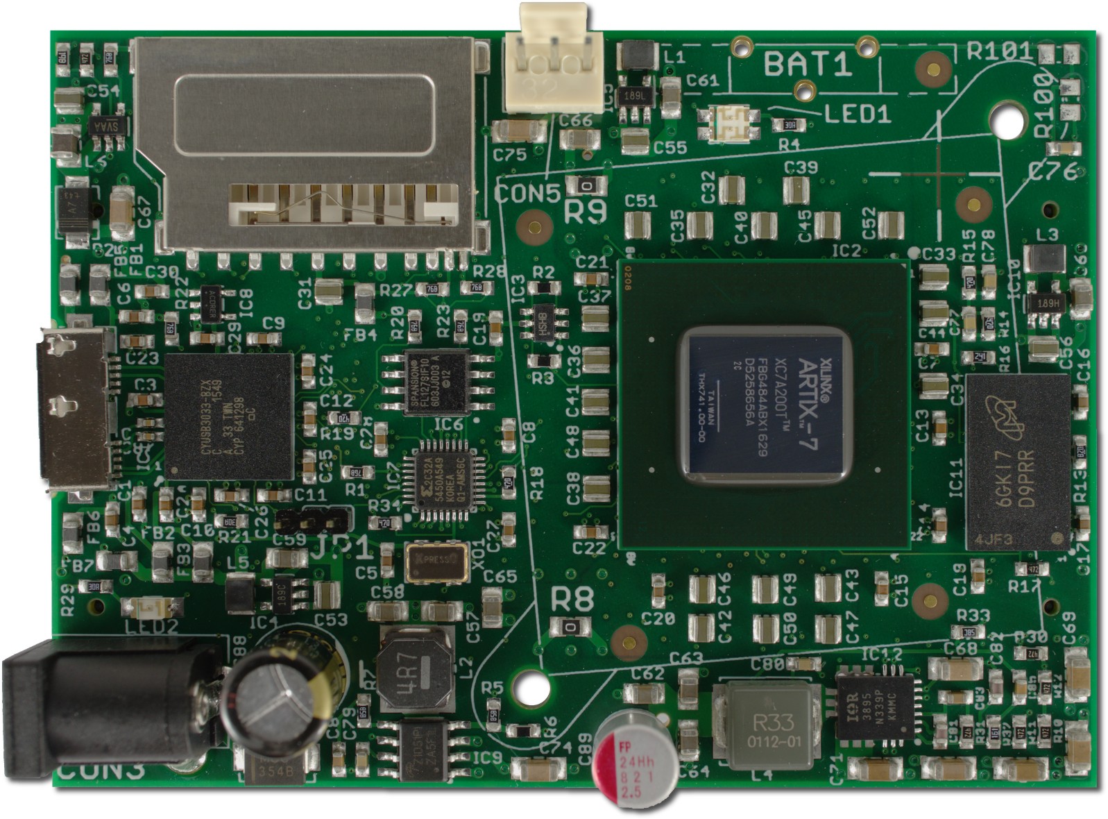
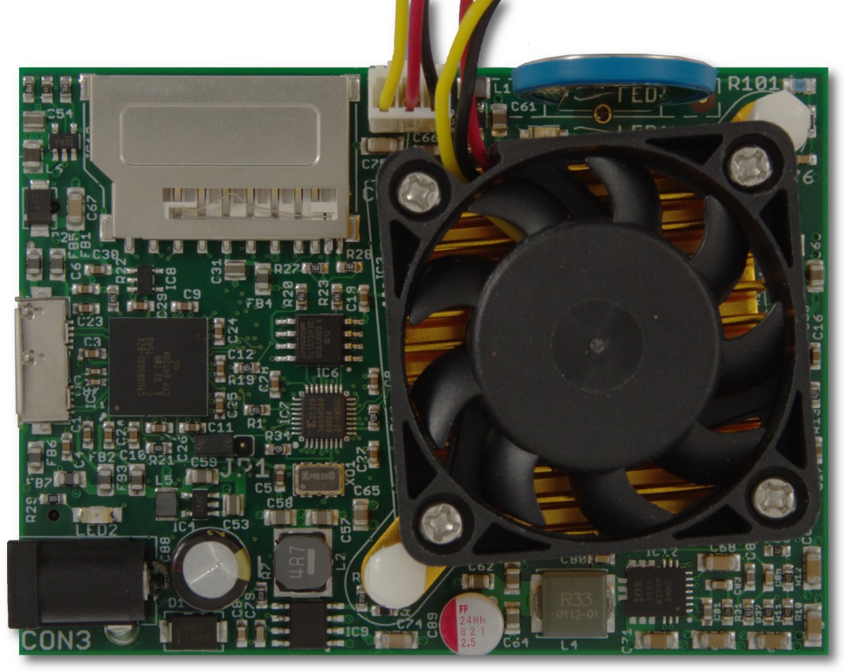
Top side of the ZTEX USB-FPGA Module 2.18 with Artix 7 XC7A200T, DDR3 SDRAM and EZ-USB FX3 USB 3.0 controller |
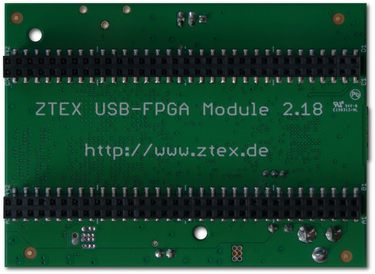
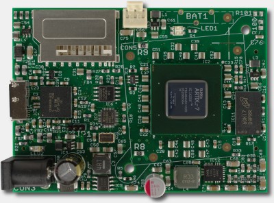
Bottom side of USB-FPGA Module 2.18 with Artix 7 XC7A200T FPGA and EZ-USB FX3. |

USB-FPGA Module 2.16 with passive (top) and active (bottom) cooler. Both heat sinks belong to the contents of delivery of the FPGA Board. |