Debug Board for Series 2 FPGA Boards
|
The Debug Board is an add-on card for Series 2 FPGA Boards. It contains a lot of LED's, switches and a JTAG header and is intended to simplify debugging and prototyping. Two variants are available.
Features
Additional resources
|
 |
Examples
The SDK contains the example "lightshow" for each Series 2 FPGA Board which demonstrates the usage of the Debug Board.
Functional description
The following sections describe the function of the three 10-LED arrays LED1-LED3, the 10 position DIP switch S1 and the layout of the prototyping area.
LED's
The LED's are connected to GPIO pins of the external I/O connector of the FPGA Board. Their connection to ground can be opened in groups of five by using a switches S1-1 to S1-6, see the schematics for details. This allows to deactivate the LED's and to use the GPIO's for in the application circuit.The GPIO usage is listed in the following table.
| LED | GPIO pin | Activation switch |
| LED1-1 | A6 | S1-1 |
| LED1-2 | B6 | |
| LED1-3 | A7 | |
| LED1-4 | B7 | |
| LED1-5 | A8 | |
| LED1-6 | B8 | S1-2 |
| LED1-7 | A9 | |
| LED1-8 | B9 | |
| LED1-9 | A10 | |
| LED1-10 | B10 | |
| LED2-1 | C3 | S1-3 |
| LED2-2 | D3 | |
| LED2-3 | C4 | |
| LED2-4 | D4 | |
| LED2-5 | C5 | |
| LED2-6 | D5 | S1-4 |
| LED2-7 | C6 | |
| LED2-8 | D6 | |
| LED2-9 | C7 | |
| LED2-10 | D7 | |
| LED3-1 | C8 | S1-5 |
| LED3-2 | D8 | |
| LED3-3 | C9 | |
| LED3-4 | D9 | |
| LED3-5 | C10 | |
| LED3-6 | D10 | S1-6 |
| LED3-7 | C11 | |
| LED3-8 | D11 | |
| LED3-9 | C12 | |
| LED3-10 | D12 |
Switches
The four remaining switches of S1 are connected to GPIO pins of the FPGA Board. In ON-position they switch the FPGA pin through a 180 Ω resistor to GND, see the schematics for details. In order to read out the switch position the FPGA pin must be internally pulled high using the PULLUP constraint.If the switches are open the GPIO pins can be used is the application circuit.
The GPIO assignment is listed in the following table.
| Switch | GPIO pin |
| S1-7 | A11 |
| S1-8 | B11 |
| S1-9 | A12 |
| S1-10 | B12 |
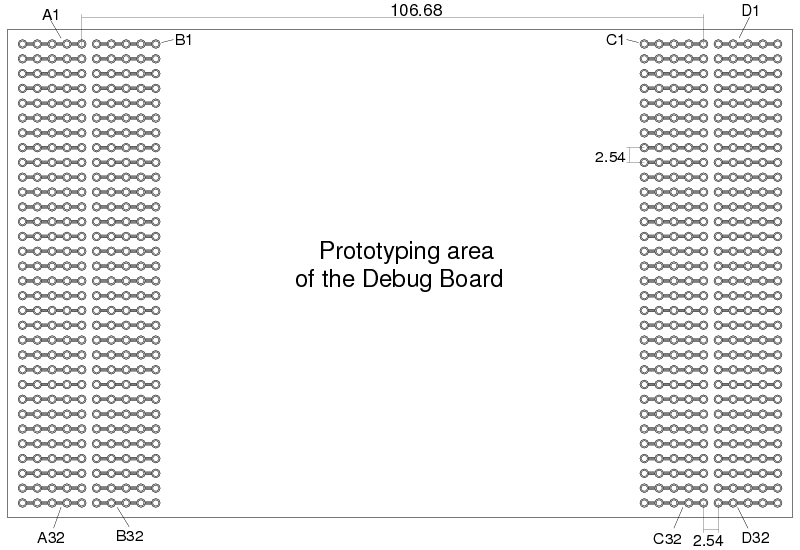
Prototyping area
The layout of the prototyping area is depicted in the following drawing. Pin assignment is the same as of Series 2 FPGA Boards (i.e. pin A1 of prototyping area is connected to A1 of FPGA board, ...).Debug Boards with prototyping area can be connected to triple-pad or other prototyping cards using two 2x32 pin headers. These parts are available in the shop.
Images
Click on the images for larger versions.
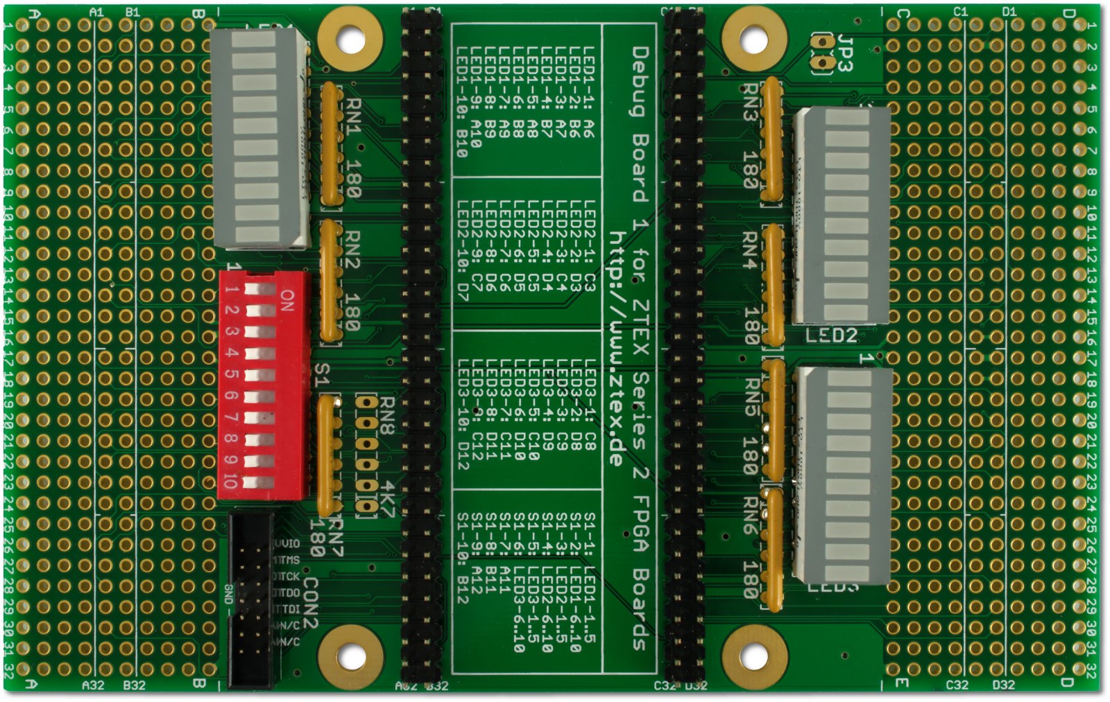
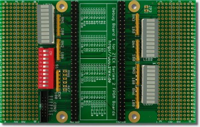
Debug Board for ZTEX Series 2 FPGA Boards: variant with prototyping area. |
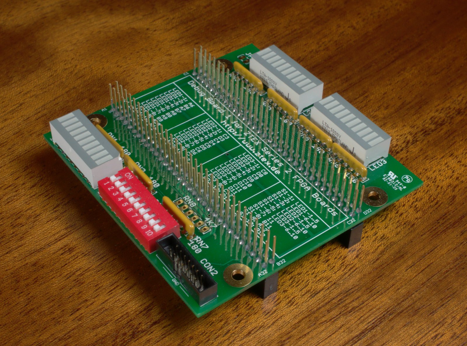
Debug Board for ZTEX Series 2 FPGA Boards: variant with stackable pin headers. |
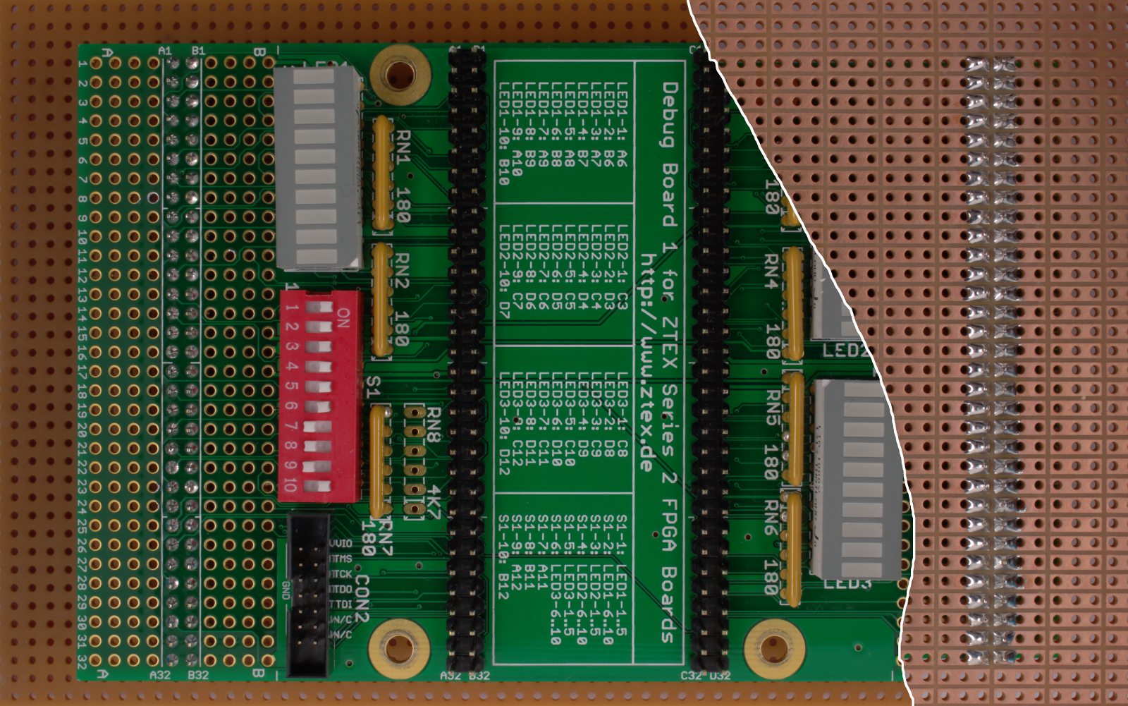
Debug Boards for ZTEX Series 2 FPGA Boards with prototyping area perfectly fit on a triple-pad Prototyping PCB's. |