Experimental Board 1.2 for Series 1 FPGA Boards
Series 1 FPGA Boards are deprecated. Please switch to Series 2.
The old product page is still available here for documentation purposes.
|
Features Additional resources |
 |
Features
- Baseboard for USB-FPGA Modules 1.2 and 1.11. (For USB-FPGA Modules 1.15 the Experimental Board 1.3 is recommended.)
- High-efficiency switching regulators to generate the supply voltages
- 1.2 V @ 2.7 A
- 2.6 V @ 2.5 A
- 3.3 V @ 2.5 A
- Wide input range: 4.5 to 16 V
- I/O voltages VCCO_IO(=VCCO_RIGHT) and VCCO_TOP can be easily and independently set to 3.3V, 2.6V, 1.2V or to an external voltage. (On Spartan 6 USB-FPGA Module 1.11 VCCO_TOP has no function. The I/O voltage of the pins at rows C,D and F of the I/O Connector is 3.3V.)
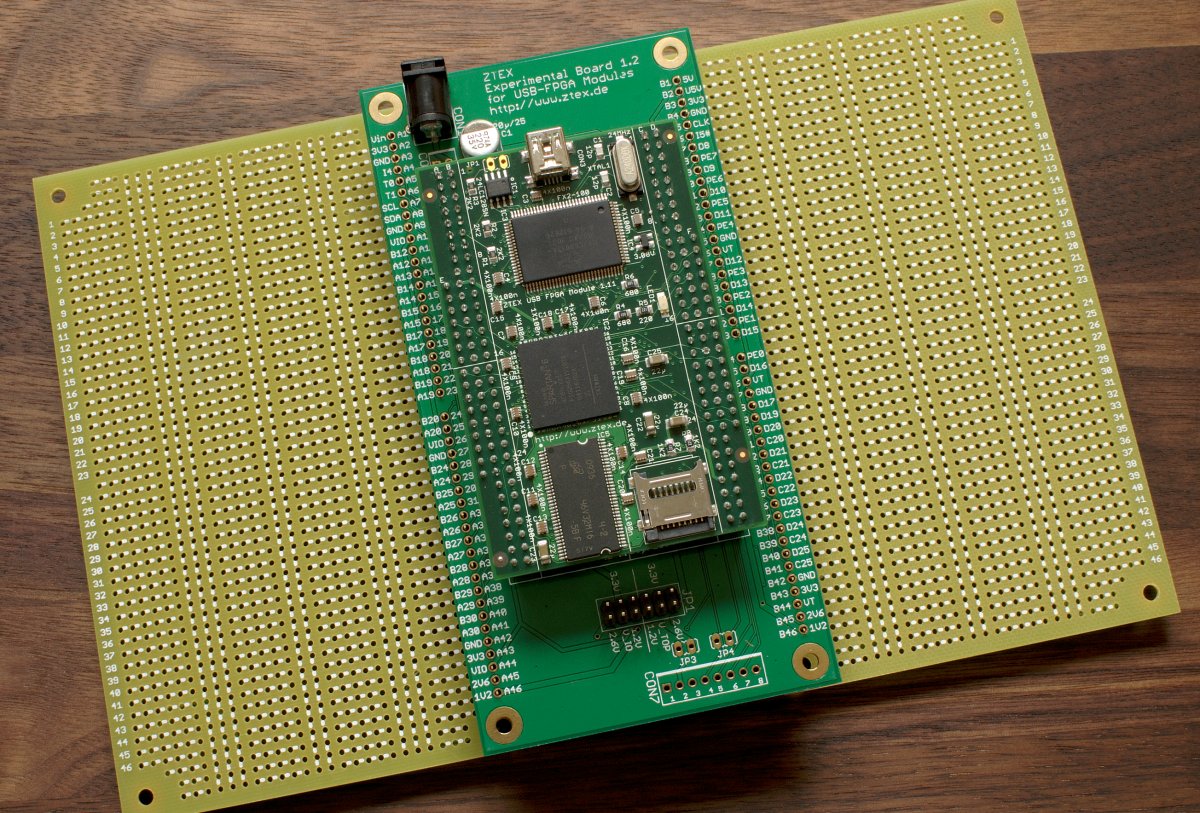
- All I/O Ports available on a standard 2.54 mm (0.1 inch) grid via four 1x23 pin and two 1x16 pin connectors to which Expansion Boards or Breadboards can be connected
- Downward pin compatible to Experimental Board 1.1
- JTAG interface for the FPGA
Functional description
The following drawing shows the measurements and the location of the of the described elements.
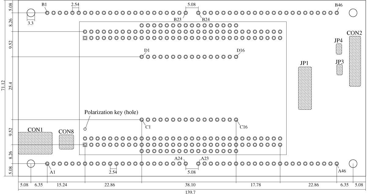
Click on the image for a larger version or download the PDF version.
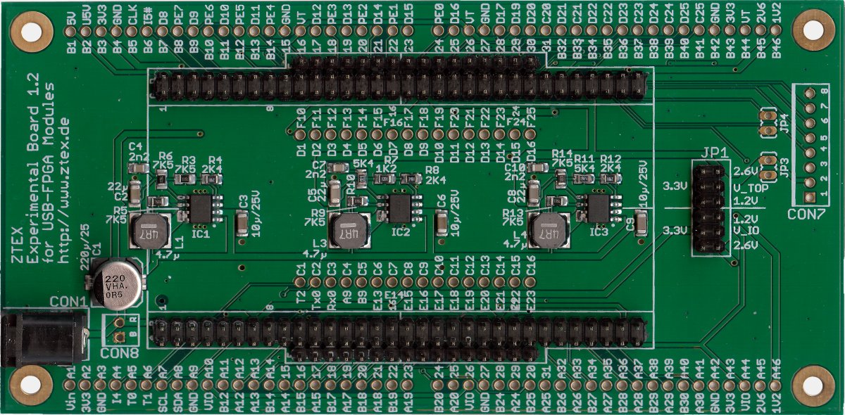
External power: CON1 and CON8
CON1 is a standard DC power jack with 2.1mm center pin (+) diameter and 5.5mm barrel (-) diameter for a supply voltage of 4.5 V to 16 V.Alternatively CON8 can be used to connect non standard power cables. The ground pin of CON8 (quadratic pad) is marked with "B" and the supply pin (oval pad) is marked with "R", see the images below.
It is also possible to supply the external voltage via the Vin Pin of the Experimental Board I/O Connector described below.
If non-stabilized power supplies are used it must be made sure that the peak voltage is not larger then 18V.
Hints for power supply via USB can be found on the ZTEX Wiki.
JTAG connector: CON7, JP3 and JP4
The pin description of the JTAG connector CON7 reads as follows:
| Pin | Description |
| 1 | +3.3V |
| 2 | +2.6V |
| 3 | Not connected |
| 4 | TMS |
| 5 | TCK |
| 6 | TDI |
| 7 | TDO |
| 8 | GND |
The voltage for the I/O signals (TCK,TMS,TDI,TDO) is 2.6V. Pin 2 can be used as supply for these signals. Pin 1 (+3.3V) can be used as supply for the JTAG adapter.
On USB-FPGA Modules 1.2 jumpers JP3 and JP4 can be closed to enforce JTAG configuration mode. But usually this is not required since the JTAG interface is always enabled. On USB-FPGA Modules 1.11 these jumpers have no function.
An appropriate connector set for CON7 is delivered with the Experimental Board.
I/O voltages: JP1
Jumper JP1 sets the I/O VCCO_IO(=VCCO_RIGHT) and VCCO_TOP, respectively. (On Spartan 6 USB-FPGA Module 1.11 V_TOP has no function. The I/O voltage of the pins at rows C,D and F of the I/O Connector is fixed to 3.3V.)By closing this jumpers (see images below) the I/O voltages can be switched easily to 3.3V, 2.6V or 1.2V. If other I/O voltages are required the jumpers must be left open and the I/O voltage must be supplied via th VIO or VT pins of the Experimental Board I/O Connector, respectively.
Experimental Board I/O Connector
Four 1x23 pin connectors (rows A and B) and two 1x16 PIN (rows C and D) connectors deliver I/O signals and voltages to user circuits. The four 1x23 pin connectors are downward pin compatible with Experimental Board 1.1. The two 1x16 pin connectors contain the additional I/O's introduced with the Spartan 6 USB-FPGA Module 1.11 and the serial interface of the EZ-USB FX2.
The drawing shows the position of the connectors.
The Pinlist and the List of Connections are can be downloaded in Gnumeric or Excel format. The following table is is a short version the these files:
| Experimental Board 1.2 | USB-FPGA Boards | |||||||
| I/O connector pin |
FX2 pin |
Spartan 3 USB-FPGA Module 1.2 FPGA pin |
Spartan 6 USB-FPGA Module 1.11 FPGA pin |
|||||
| Pin | Pin name | |||||||
| A1 | Vin | |||||||
| A2 | 3V3 | |||||||
| A3 | GND | |||||||
| A4 | I4 | A3 | 22 | |||||
| A5 | T0 | B3 | 23 | |||||
| A6 | T1 | A4 | 24 | |||||
| A7 | SCL | A6 | 29 | |||||
| A8 | SDA | B6 | 30 | |||||
| A9 | GND | B13 | ||||||
| A10 | VIO | |||||||
| A11 | B12 | B12 | 73 | B14 | ||||
| A12 | A12 | A12 | 74 | A14 | ||||
| A13 | A13 | A13 | 76 | C13 | ||||
| A14 | B14 | B14 | 77 | D11 | ||||
| A15 | A14 | A14 | 78 | D12 | ||||
| A16 | B15 | B15 | 79 | F10 | ||||
| A17 | A15 | A15 | 80 | E11 | ||||
| A18 | B17 | B17 | 82 | E10 | ||||
| A19 | A17 | A17 | 83 | C10 | ||||
| A20 | B18 | B25 | 95 | F7 | ||||
| A21 | A18 | A18 | 85 | B12 | ||||
| A22 | B19 | B19 | 86 | C9 | ||||
| A23 | A19 | A19 | 87 | A9 | ||||
| A24 | B20 | B20 | 89 | D8 | ||||
| A25 | A20 | A20 | 90 | C8 | ||||
| A26 | VIO | |||||||
| A27 | GND | |||||||
| A28 | B24 | B24 | 92 | C7 | ||||
| A29 | A24 | A24 | 93 | A7 | ||||
| A30 | B25 | B18 | 84 | A12 | ||||
| A31 | A25 | A25 | 96 | E6 | ||||
| A32 | B26 | B26 | 97 | D6 | ||||
| A33 | A26 | A26 | 98 | C6 | ||||
| A34 | B27 | B27 | 99 | B6 | ||||
| A35 | A27 | A27 | 100 | A6 | ||||
| A36 | B28 | B28 | 102 | D5 | ||||
| A37 | A28 | A28 | 103 | C5 | ||||
| A38 | B29 | B29 | 104 | B5 | ||||
| A39 | A29 | A29 | 105 | A5 | ||||
| A40 | B30 | B30 | 107 | C4 | ||||
| A41 | A30 | A30 | 108 | A4 | ||||
| A42 | GND | |||||||
| A43 | 3V3 | |||||||
| A44 | VIO | |||||||
| A45 | 2V5 | |||||||
| A46 | 1V2 | |||||||
| B1 | 5V | |||||||
| B2 | U5V | |||||||
| B3 | 3V3 | |||||||
| B4 | GND | |||||||
| B5 | CLK | C3 | 52 | R16 | ||||
| B6 | I5# | C5 | 84 | |||||
| B7 | D8 | D8 | 5 | K16 | ||||
| B8 | PE7 | C9 | 93 | |||||
| B9 | D9 | D9 | 4 | L16 | ||||
| B10 | PE6 | C10 | 92 | |||||
| B11 | D10 | D10 | 2 | M16 | ||||
| B12 | PE5 | C11 | 91 | |||||
| B13 | D11 | D11 | 1 | P16 | ||||
| B14 | PE4 | C12 | 90 | |||||
| B15 | GND | |||||||
| B16 | VT | |||||||
| B17 | D12 | D12 | 141 | P15 | ||||
| B18 | PE3 | C13 | 89 | |||||
| B19 | D13 | D13 | 140 | T15 | ||||
| B20 | PE2 | C14 | 88 | |||||
| B21 | D14 | D14 | 137 | K15 | ||||
| B22 | PE1 | C15 | 87 | |||||
| B23 | D15 | D15 | 135 | R14 | ||||
| B24 | PE0 | C16 | 86 | |||||
| B25 | D16 | D16 | 132 | M13 | ||||
| B26 | VT | |||||||
| B27 | GND | |||||||
| B28 | D17 | D17 | 131 | M12 | ||||
| B29 | D19 | D19 | 130 | T12 | ||||
| B30 | D20 | D20 | 129 | R9 | ||||
| B31 | C20 | C20 | 128 | P8 | ||||
| B32 | D21 | D21 | 127 | N9 | ||||
| B33 | C21 | C21 | 125 | M9 | ||||
| B34 | D22 | D22 | 124 | N8 | ||||
| B35 | C22 | C22 | 123 | T7 | ||||
| B36 | D23 | D23 | 122 | P7 | ||||
| B37 | C23 | C23 | 119 | M7 | ||||
| B38 | D24 | D24 | 118 | P6 | ||||
| B39 | C24 | C24 | 116 | N6 | ||||
| B40 | D25 | D25 | 113 | P4 | ||||
| B41 | C25 | C25 | 112 | M6 | ||||
| B42 | GND | |||||||
| B43 | 3V3 | |||||||
| B44 | VT | |||||||
| B45 | 2V5 | |||||||
| B46 | 1V2 | |||||||
| C1 | T2 | B4 | 25 | |||||
| C2 | Tx0 | A8 | 40 | |||||
| C3 | Rx0 | B8 | 41 | |||||
| C4 | A9 | A9 | B15 | |||||
| C5 | B9 | B9 | B16 | |||||
| C6 | E13 | E13 | A13 | |||||
| C7 | E14 | E14 | C11 | |||||
| C8 | E15 | E15 | A11 | |||||
| C9 | E16 | E16 | B10 | |||||
| C10 | E17 | E17 | A10 | |||||
| C11 | E18 | E18 | F9 | |||||
| C12 | E19 | E19 | D9 | |||||
| C13 | E20 | E20 | A8 | |||||
| C14 | E21 | E21 | B8 | |||||
| C15 | E22 | E22 | E8 | |||||
| C16 | E23 | E23 | E7 | |||||
| D1 | F10 | F10 | N16 | |||||
| D2 | F11 | F11 | M15 | |||||
| D3 | F12 | F12 | R15 | |||||
| D4 | F13 | F13 | L14 | |||||
| D5 | F14 | F14 | N14 | |||||
| D6 | F15 | F15 | L13 | |||||
| D7 | F16 | F16 | L12 | |||||
| D8 | F17 | F17 | R12 | |||||
| D9 | F18 | F18 | M11 | |||||
| D10 | F19 | F19 | M10 | |||||
| D11 | F20 | F20 | T9 | |||||
| D12 | F21 | F21 | P9 | |||||
| D13 | F22 | F22 | T8 | |||||
| D14 | F23 | F23 | R7 | |||||
| D15 | F24 | F24 | T6 | |||||
| D16 | F25 | F25 | T4 | |||||
PMOD connectors
PMOD modules can be connected directly to the following positions of the Experimental Board I/O connector:- A26 - A31
- A43 - A38
- B43 - B38
- B26 - B31
- B16 - B11
Compatibility notes
Depending on the application the Experimental Board 1.2 may not deliver enough current for USB-FPGA Modules 1.15. For these Boards the Experimental Board 1.3 is recommended.Users switching from Experimental Board 1.1 have to consider the following differences:
- The Experimental Board 1.2 does not contain serial drivers anymore. The serial port signals form the EZ-USB FX2 are now available on pins C2 to C5 of the Experimental Board I/O Connector
- Functions of pins A20 and A30 have been swapped. (Users of USB-FPGA Modules 1.2 have to swap pins 95 and 84 of the FPGA in the ucf file. Users of Spartan 6 USB-FPGA Modules 1.11 have to swap pins F7 and A12 of the FPGA in the ucf file.)
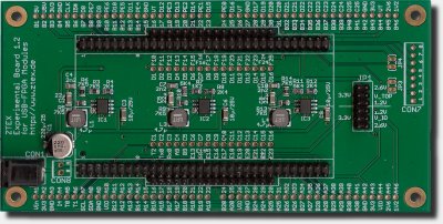
Images
Click on the images for larger versions.
Development Board / Experimental Board 1.2. |
Experimental Board with Spartan 6 USB-FPGA Module 1.11 and two Expansion Boards.
|
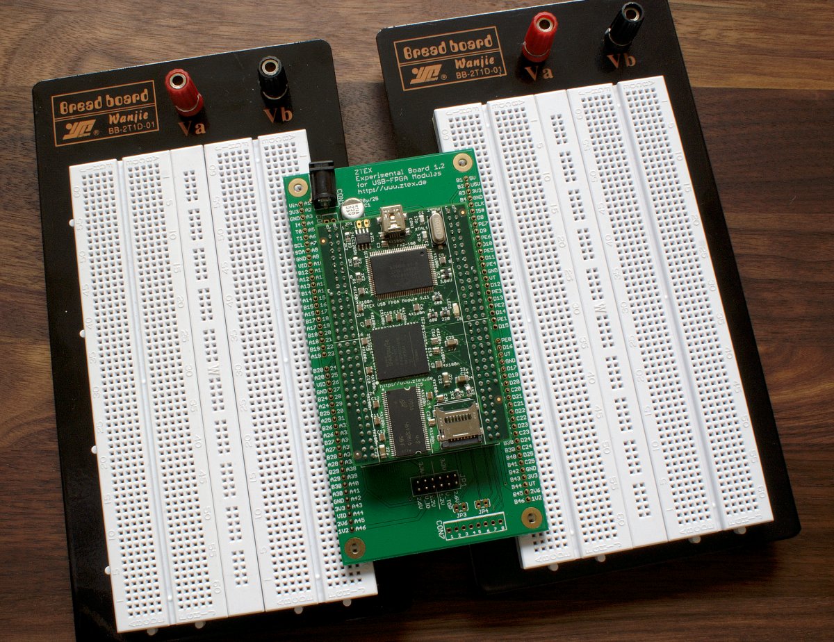
Experimental Board with Spartan 6 USB-FPGA Module 1.11 and two Breadboards.
|