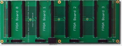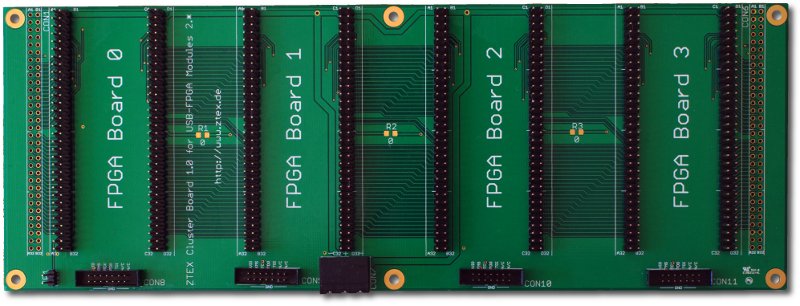
Cluster Base Board for ZTEX Series 2 FPGA Boards
|
The Cluster Base Board connects four Series 2 FPGA Boards to a small cluster node. Features
|
 |
Functional description
External I/O connectors are named CON1 and CON6. Their pin assignment if listed in the table below. Positions of the components which are de described here can be found in the measurements file.
Net list
Each row in the header of the table below lists components that are connected together. The rows in the table body shows which pins of the parts are connected together.
Here are a few examples how the table is read:
- B8 of CON1 is connected to B6 of FPGA Board 0
- B8 of CON6 is connected to D6 of FPGA Board 3
- B6 of Board 1 is connected to D6 of Board 0
- BUS[0] is connected to A3 of CON1/CON6 and to B3 of Boards 0-3
CON1
PWR
Bus
Board 0
Bus
Board 1
Board 0
Bus
Board 2
Board 1
Bus
Board 3
Board 2
CON6
PWR
Bus
Board 3
A1
VIN
B1
VIN
A2
GND
B2
GND
A3
BUS[0]
B3
B3
BUS[1]
C3
A4
BUS[2]
A4
B4
BUS[3]
B4
A5
BUS[4]
C4
B5
BUS[5]
D4
A6
BUS[6]
A5
B6
BUS[7]
B5
A7
BUS[8]
C5
B7
BUS[9]
D5
A8
A6
C6
B8
B6
D6
A9
A7
C7
B9
B7
D7
A10
A8
C8
B10
B8
D8
A11
A9
C9
B11
B9
D9
A12
A10
C10
B12
B10
D10
A13
A11
C11
B13
B11
D11
A14
A12
C12
B14
B12
D12
A15
A13
C13
B15
B13
D13
A16
A14
C14
B16
B14
D14
CON1
PWR
Bus
Board 0
Bus
Board 1
Board 0
Bus
Board 2
Board 1
Bus
Board 3
Board 2
CON6
PWR
Bus
Board 3
A17
A18
C15
B17
B18
D15
A18
A19
C19
B18
B19
D19
A19
A20
C20
B19
B20
D20
A20
A21
C21
B20
B21
D21
A21
A22
C22
B21
B22
D22
A22
A23
C23
B22
B23
D23
A23
A24
C24
B23
B24
D24
A24
A25
C25
B24
B25
D25
A25
A26
C26
B25
B26
D26
A26
A27
C27
B26
B27
D27
A27
A28
C28
B27
B28
D28
A28
A29
C29
B28
B29
D29
A29
A30
C30
B29
B30
D30
A30
GND
B30
GND
A31
VIO
B31
VIO
A32
3.3V
B32
3.3V
Board ID pins
The pins D3 and A3 of each FPGA Board are used as board ID as follows:
| A3 | D3 | |
|---|---|---|
| Board 0 | 0 | 0 |
| Board 1 | 0 | Z |
| Board 2 | Z | 0 |
| Board 3 | Z | Z |
Z means that the pin is floating. In order to read the ID out the pins have to be internally pulled up (using the PULLUP constraint).
External Power Supply
The VIN pins of the two external I/O connectors and all FPGA Boards are connected to a bus. This means that all FPGA Boards must be driven by the same power supply. But this also allows to supply the cluster node centrally either by using the pluggable terminal CON7 or by using the DC connector of one of the FPGA Boards. The usage of CON7 is recommended because this connector is designed for large currents. The terminal block is delivered with the Cluster Base Board and has three contacts. The two outer ones are GND (-) and the central one is the supply voltage (+).
JTAG headers
Four standard 14 pin JTAG headers are installed. Each one is connected to the FPGA Board which is next to it.
I/O voltages
The 0 Ω resistors R1 to R3 (1206 packages) can be installed if some of the FPGA boards have I/O voltage pins that are configured as inputs. By default all of them are outputs and therefore R1 to R3 should be open. See the schematics and the FPGA Board description for details.
Pins A31 and B31 of the external I/O connector CON1 are connected to VCCO_AB of the first FPGA Board and A31 and B31 of CON6 are connected to VCCO_CD of the last FPGA Board. By default these pins are 3.3V outputs. If another I/O voltage than 3.3V is desired the 0 Ω resistor on the FPGA Board which connects VCCO_AB or VCCO_CD with 3.3V has to be removed and the I/O voltage has to be supplied through pins A31 and B31 of CON1 or CON6, respectively. See the FPGA Board description for details.
Reset: JP1
Closing jumper JP1 hard-resets all FPGA Boards.
Images
Click on the images for larger versions.

Cluster Base Board for four ZTEX Series 2 FPGA Boards |