Power Supply Module 1.0 for Series 1 FPGA Boards
Series 1 FPGA Boards are deprecated. Please switch to Series 2.
The old product page is still available here for documentation purposes.
|
Features Additional resources |
 |
Features
- Power Supply Board for USB-FPGA Modules 1.2 and 1.11. (For USB-FPGA Modules 1.15 the Power Supply Module 1.1 is recommended.)
- Wide input range: 8 to 25 V
- Delivers all required voltages using high-efficiency step down regulators:
- 1.2 V @ 1.6 A (3 A peak)
- 2.5 V @ 1.6 A (3 A peak)
- 3.3 V @ 1.6 A (3 A peak)
- I/O voltages VCCO_RIGHT / VCCO_IO and VCCO_TOP can be easily and independently set to 3.3V, 2.5V or to an external voltage. (On Spartan 6 USB-FPGA Module 1.11 VCCO_TOP has no function. The I/O voltage of the pins at rows C,D and F of the I/O Connector is 3.3V.)
- JTAG interface for the FPGA
Functional description
The following drawing shows the measurements and the location of the of the described elements.
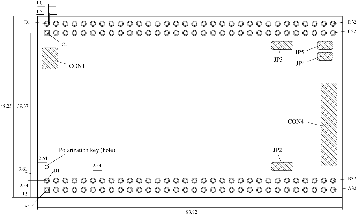
Click on the image for a larger version or download the PDF version.
External power: CON1
Connector CON1 is used to supply an external 8 to 25 V voltage. The ground pin (quadratic pad) is marked by "-" and "B" and the supply pin (oval pad) is marked by "+" and "R", see the images below.An appropriate power connector set consisting of a male 2 pin header and a female 2 pin connector with cable is delivered together with the Power Supply Module.
I/O voltages: JP2, JP3
The middle pin of jumpers JP2 and JP3 can be used to supply the I/O voltages VCCO_RIGHT / VCCO_IO and VCCO_TOP, respectively, see images below. By closing this jumpers (see images below) the I/O voltages can be switched easily to 3.3V or 2.5V. (On Spartan 6 USB-FPGA Module 1.11 VCCO_TOP has no function. The I/O voltage of the pins at rows C,D and F of the I/O Connector is 3.3V.)JTAG connector: CON4, JP4, JP5
The pin description of the JTAG connector CON4 reads as follows:
| Pin | Description |
| 1 | +3.3V |
| 2 | +2.5V |
| 3 | Not connected |
| 4 | TMS |
| 5 | TCK |
| 6 | TDI |
| 7 | TDO |
| 8 | GND |
The voltage for the I/O signals (TCK,TMS,TDI,TDO) is 2.5V. Pin 2 can be used as supply for these signals. Pin 1 (+3.3V) can be used as supply for the JTAG adapter.
The JTAG mode of the FPGA can be enforced by closing jumpers JP4 and JP5. But usually this is not required, i.e. JTAG configuration works even if these jumpers are open.
An appropriate power connector set for CON4 is delivered with the Power Supply Module.
[TOC]
Package contents
|

|
Images
Click on the images for larger versions.
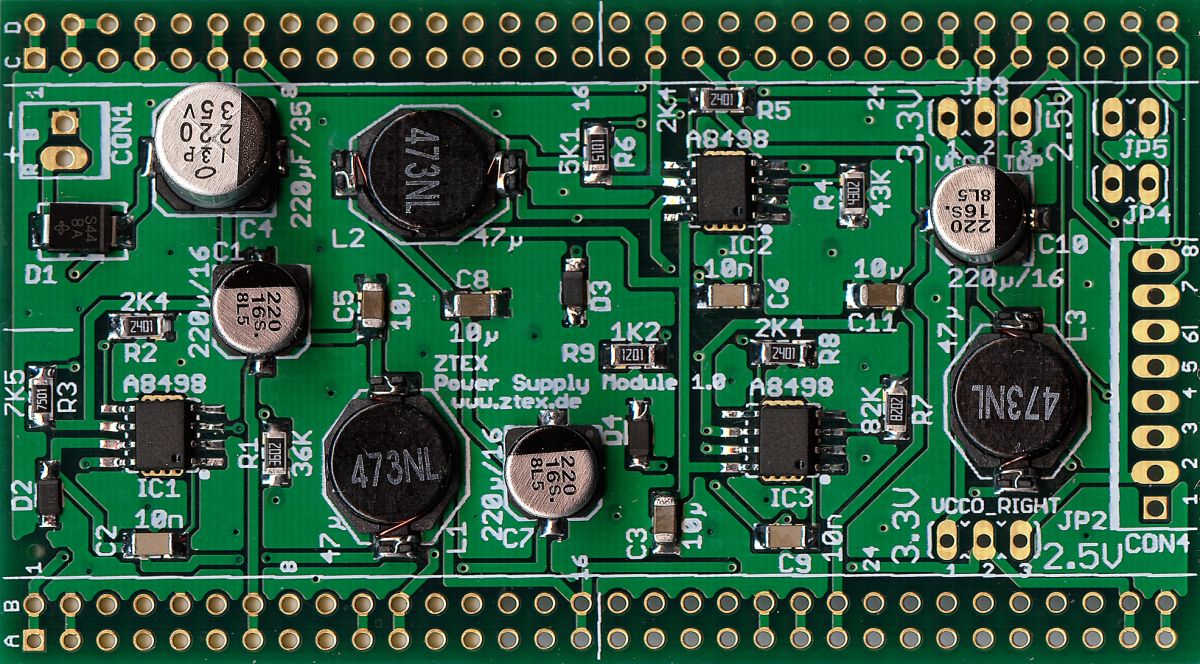
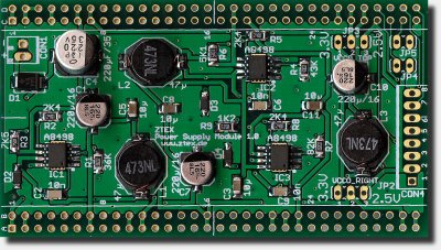
Top side of the Power Supply Module. |
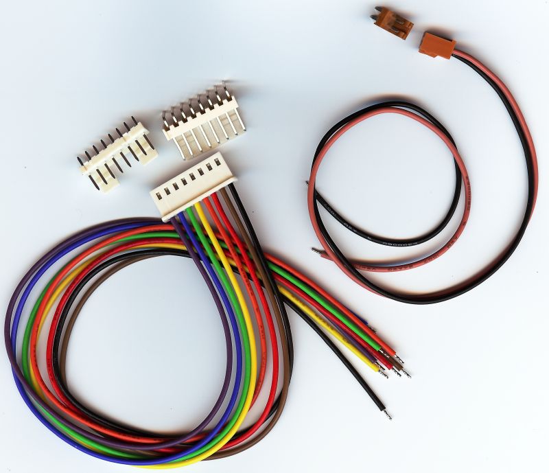
Accessories delivered with the Power Supply Power Supply Module. |
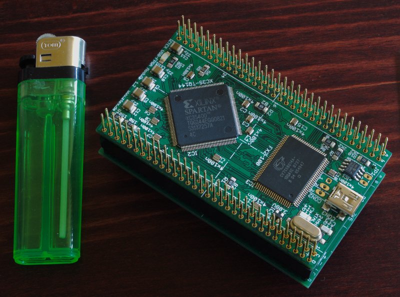
USB-FPGA Module 1.2 stacked on a Power Supply Module.
|
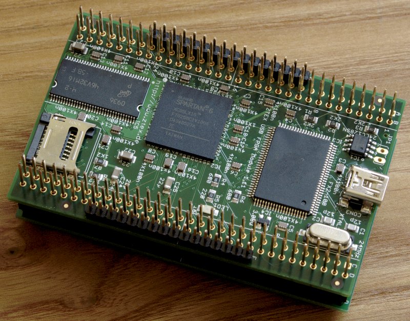
Spartan 6 USB-FPGA Module 1.11 stacked on a Power Supply Module.
|