USB-FPGA Module 1.15:
Spartan 6 LX45, LX75 and LX150 FPGA Board with USB 2.0 Microcontroller and 128 MByte DDR2 SDRAM
USB-FPGA Modules 1.15 are deprecated. Please switch to Series 2 FPGA Boards.
An Adapter is available as workaround.
The old product page is still available here for documentation purposes.
|
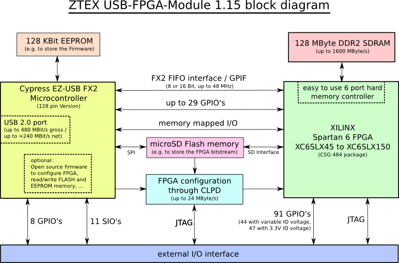
Block diagram
Schematics (PDF) |
 |
Block diagram
Features
- High-Speed (480 MBit/s) USB interface via Mini-USB connector (B-type)
- Cypress CY7C68013A EZ-USB FX2 Microcontroller
- Four Xilinx Spartan 6 FPGA variants: LX45 (XC6SLX45), LX75 (XC6SLX75), LX100 (XC6SLX100) and LX150 (XC6SLX150) FPGA, see Variants
-
99 General Purpose I/O's (GPIO):
- 91 FPGA GPIO's
- 8 EZ-USB FX2 GPIO's
-
15 special I/O's (SIO):
- 4 pins for FPGA configuration via JTAG
- 2 pins for 1 serial ports
- 2 pins I2C interface (2 pins)
- 2 interrupt pins
- 3 timers
- 1 Wakeup pin
- 1 Breakpoint pin
-
128 MByte DDR2 SDRAM:
- Up to 400 MHz clock frequency
- 16 Bit bus width
- Up to 1600 MByte/s data rate
- Easy to use hard memory controller included Spartan 6 FPGA with 6 ports. (see SDK for examples)
- MicroSD socket for extensible Flash memory (standard and high capacity (SDHC) cards, SPI mode support required)
-
Fast FPGA configuration using CPLD:
- Up to 24 MByte/s via USB
- Up to 2.5 MByte/s from microSD Flash (depends on the speed of the card)
- Memory mapped IO between EZ-USB FX2 and FPGA
- 128 Kbit EEPROM memory (can be used to store the EZ-USB firmware)
- 2 Kbit MAC-EEPROM: contains a unique non erasable MAC-address
- External power supply required:
- 3.3 V; supply current depends on application (see Spartan 6 datasheets), recommended: ≥ 800 mA
- 2.5 V - 2.6 V; supply current depends on application (see Spartan 6 datasheets), recommended: ≥ 300 mA
- 1.2 V; supply current depends on application (see Spartan 6 datasheets), see the variants table for recommended minimum currents
- Variable I/O voltage VCCO_IO: 1.14...3.46 V; supply current depends on application (see Spartan 6 datasheets), recommended: ≥ 500 mA
- Heat sink for high performance / high speed applications, see Section heat sink
- No soldering required: Female pin headers on bottom side (two 2x32 und two 1x23)
- Temperature range: 0-70°C (-25°C - 85°C on request)
- FPGA configuration / programming via USB using the EZ-USB FX2 SDK. (No JTAG adapters or other additional utilities required.)
- FPGA configuration / programming from Flash memory
Variants
Variants with different features are offered:
| Variant | FPGA | Speed grade (larger means faster) |
Recommended minimum current of 1.2V supply |
Max. memory clock / bandwidth |
Availability |
| USB-FPGA Module 1.15a | XC6SLX45 | 3 | 1800 mA | 333 MHz / 1333 MByte/s | Out of stock, please switch to Series 2 FPGA Boards |
| USB-FPGA Module 1.15b | XC6SLX75 | 3 | 3000 mA | 400 MHz / 1600 MByte/s | |
| USB-FPGA Module 1.15c | XC6SLX100 | 3 | 4000 mA | 400 MHz / 1600 MByte/s | |
| USB-FPGA Module 1.15d | XC6SLX150 | 3 | 6000 mA | 400 MHz / 1600 MByte/s |
Other variants (with or without pin headers, other speed grades, extended temperature range) can be produced on request. The LX75 FPGA Board (1.15b) is the largest variant which is supported by the free ISE Webpack version. 1.15c (XC6SLX100) and 1.15d (XC6SLX150) variants require a non-free license or a free 30 day evaluation license.
SDK, Examples, Getting Started
A powerful open source Firmware Development Kit with platform independent host software API is available for the FPGA Board. This SDK allows to define all USB device descriptors using only a few macro commands, and thus gives the developer a quick start into Firmware programming.The SDK package contains a lot of examples which can be used as starting point for own applications.
More Information are available in the EZ-USB FX2 SDK section.
Additional documentation including Tutorials can also be found on the ZTEX Wiki
Functional description
The following drawing shows the measurements and the location of the of the described elements.

Click on the image for a larger version or download the PDF version.
FPGA configuration
There are three ways to configure the FPGA:- From USB with the SDK. This can be done using the API (see configureFpga) or using the utilities FWLoader or DeviceServer. DeviceServer allows comfortable access to the FPGA Board using the http interface and your Web browser as GUI.
- Via JTAG, see JTAG section below. Bitstream upload to large FPGA's (like XC6SLX150) via JTAG may take quite long. Therefore the USB method should be preferred.
- From microSD, see the standalone description on the ZTEX Wiki.
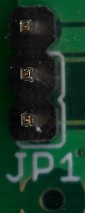
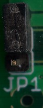
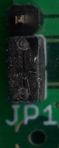
EEPROM address: JP1
Jumper JP1 specifies the I2C address of the EEPROM:
| JP1 | I2C address |
| open | 0xA2 |
| close | 0xAA |
The EZ-USB FX2 Microcontroller searches for the firmware at the address 0xA2 which is the default address (jumper open).
The main purpose of this jumper is to disable EEPROM boot-loading. If, for example, the EEPROM was programmed with a corrupt firmware the Microcontroller can be booted with the internal firmware by closing JP1 during powering-on the FPGA Board.
JP1 has an unconnected pin which can be used for parking the jumper. The following pictures show all possible jumper positions:
|
|
| JP1 open | JP1 closed |
FPGA state: LED1
LED1 indicates the configuration state of the FPGA as follows:
| LED1 | FPGA |
| on | unconfigured |
| off | configured |
Clock resources
On the FPGA board two clocks sources are connected to the FPGA: the clock output of the EZ-USB FX2 which is usually configured to 48 MHz and the interface clock which can be configured to 30 MHz or to 48 MHz. They can be used to generate new clocks within the FPGA using DCM's or PLL's.Additional clocks can be connect to the GCLK pins of the I/O connector.
In most cases the on board clock sources are sufficient.
Configuration booster CPLD
The CPLD allows high speed configuration of the FPGA via USB (up to 24 MByte/s) and from Flash (up to 2.5 MByte/s). The CPLD occupies Bits 0 and 3 of port A of the EZ-USB FX2.For high speed configuration via USB an output Endpoint of the EZ-USB FX2 is required. The Firmware allows to (re-)use an endpoint which is intended for user defined communication. If all Endpoint buffers of the EZ-USB FX2 are required for input Endpoints standard speed (about 1 MByte/s) configuration via Endpoint 0 has to be used.
The FPGA configuration from Flash is done in serial mode at a frequency of 24 MHz. Due to the the sector load latencies the maximum configuration speed in this mode is about 2.5 MByte/s.
The CPLD is factory programmed. Re-programming via JTAG is possible. The sources files and jed file can be downloaded here: usb-fpga-1.15-cpld.zip.
I/O Connector
Two 2x32 pin and two 1x23 pin connectors deliver the I/O signals and are used for the power supply. The drawing shows the position of these connectors.
The I/O connector of the Spartan 6 USB-FPGA Module 1.15 is mechanical downward compatible to the I/O Connector of the USB-FPGA Module 1.11 and USB-FPGA Module 1.2.
There is a polarization key in form of a small hole close to the B1 pin as shown on the drawing. In order to prevent damage equal orientation of the polarization key (hole) of all stacked boards must be ensured.
JTAG
The FPGA can be configured either via USB or via JTAG. JTAG signals are available at Pins D29 to D32 of the I/O connector. On the Experimental Board and the Power Supply Module JTAG signals are provided at 14 pin Xilinx header.
If the JTAG interface is used for FPGA configuration bit 1 of port A (=PROG_B at FPGA) must be driven high. This happens automatically if a firmware developed with the SDK is running.
The JTAG interface can also be used for re-programming the CPLD.
Heat Sink
For high performance / high speed applications a heat sink is required.The FPGA boards are delivered with a 18×18×10mm heat sink (XC6SLX45 and XC6SLX75 FPGA boards) or a 25×25×12.5mm (XC6SLX100 and XC6SLX150 FPGA boards) heat sink plus two strong double-sided thermal adhesive pads. In order to prevent damage during the shipping, the heat sinks are delivered unmounted. The recommended mounting and removal procedure is different for the two heat sink variants.
Mounting recommendation for 18×18mm heat sinks (LX45 and LX75 FPGA Boards)
- Remove the protective liner from one side of the thermal pad and apply it to the heat sink
- If desired: cut off the overhanging edges using a scissor or a sharp knife. (The thermal pad is two 2mm larger than the heat sink.)
- Remove the remaining protective liner from thermal pad and position the heat sink on the FPGA with moderate pressure
Mounting instructions for 25×25mm heat sinks (LX100 and LX150 FPGA Boards)
- Remove the protective liner from one side of the thermal pad and apply it centrical to the heat sink. Since the thermal pad is 2mm larger than the FPGA it does not need to be positioned exactly.
- Remove the protective liner from the other side position the heat sink on the FPGA with moderate pressure. Make sure that enough space is left near the microSD socket and the C5 is not contacted as depicted below.
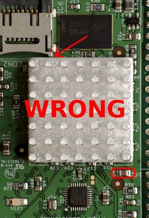 wrong |
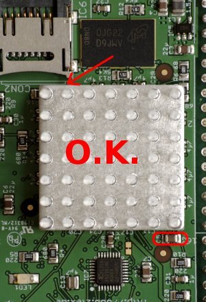 O.K. |
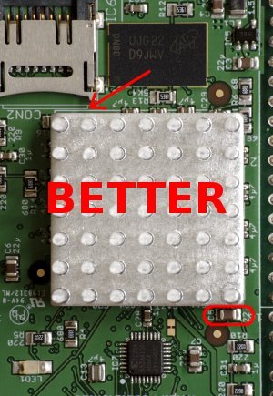 better |
Removal instructions for 18×18mm heat sinks (LX45 and LX75 FPGA Boards)
18×18mm heat sinks can be safely removed by raising up one corner using a thin blade knife.
Removal instructions for 25×25mm heat sinks (LX100 and LX150 FPGA Boards)
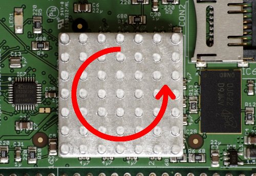
Removal of 25×25mm heat sinks is difficult and may cause damage on the board. Never pull up or lever up the heat sink. The safest way to remove the heat sink is by applying shear forces e.g. by twisting the heat sink as depicted below.
Pinlist and List of Connections
The Pinlist of the I/O Connector and the List of Connections can be downloaded in Gnumeric or Excel format. These files contain the data for all USB-FPGA Boards including compatibility information. (Attention: The files contain several sheets.)
This is the Pinlist of the I/O Connector:
Pinlist
E
A
B
C
D
F
1
4..35V
4..35V
USB_5V
USB_5V
1
2
GND
GND
5V (unused)
5V (unused)
2
3
INT4
T0
L20~IO_L43P_GCLK5_M1DQ4_1
5V (unused)
3
4
T1
T2
GND
GND
4
5
BKPT
GND
INT5#
WAKEUP*
5
6
SCL
SDA
3.3V
3.3V
6
7
3.3V
3.3V
7
8
TxD0
RxD0
GND
V20~IO_L71N_1
8
9
A20~IO_L16N_1
A19~IO_L16P_1
PE7/GPIFADR8
Y22~IO_L59N_1
9
10
1.2V
2.5V
2.5V
PE6/T2EX
AA22~IO_L63N_1
AA21~IO_L63P_1
10
11
1.2V
1.2V
1.2V
PE5/INT6
Y21~IO_L59P_1
AB21~IO_L61N_1
11
12
VREF
A18~IO_L66N_SCP0_0
B18~IO_L66P_SCP1_0
PE4/RXD1OUT
W20~IO_L53P_1
Y20~IO_L67N_1
12
13
C16~IO_L65N_SCP2_0
D17~IO_L65P_SCP3_0
GND
PE3/RXD0OUT
AA20~IO_L61P_1
AB20~IO_L65N_1
13
14
B16~IO_L63P_SCP7_0
A17~IO_L64N_SCP4_0
C17~IO_L64P_SCP5_0
PE2/T2OUT
V19~IO_L71P_1
AB19~IO_L65P_1
14
15
A16~IO_L63N_SCP6_0
C14~IO_L46N_0
D15~IO_L46P_0
PE1/T1OUT
Y19~IO_L67P_1
AB18~IO_L2N_CMPMOSI_2
15
16
B12~IO_L36P_GCLK15_0
3.3V
3.3V
PE0/T0OUT
V18~IO_L73N_1
AA18~IO_L2P_CMPCLK_2
16
17
A12~IO_L36N_GCLK14_0
A11~IO_L35N_GCLK16_0
C11~IO_L35P_GCLK17_0
GND
Y15~IO_L5P_2
AA16~IO_L4P_2
17
18
B14~IO_L50P_0
C13~IO_L48P_0
A13~IO_L48N_0
2.5V
2.5V
AB15~IO_L5N_2
18
19
A14~IO_L50N_0
C12~IO_L37N_GCLK12_0
D11~IO_L37P_GCLK13_0
1.2V
V15~IO_L13N_D10_2
W14~IO_L16P_2
19
20
D12~IO_L47N_0_NC45
C15~IO_L62P_0
F10~IO_L38P_0
Y11~IO_L31P_GCLK31_D14_2
W15~IO_L14P_D11_2
Y16~IO_L14N_D12_2
20
21
D13~IO_L47P_0_NC45
GND
GND
AA12~IO_L30P_GCLK1_D13_2
AA14~IO_L15P_2
AB14~IO_L15N_2
21
22
A10~IO_L34N_GCLK18_0
VCCO_IO
VCCO_IO
Y10~IO_L29N_GCLK2_2
AB12~IO_L30N_GCLK0_USERCCLK_2
AB11~IO_L31N_GCLK30_D15_2
22
23
B10~IO_L34P_GCLK19_0
1.2V
1.2V
AB10~IO_L32N_GCLK28_2
AA10~IO_L32P_GCLK29_2
W11~IO_L29P_GCLK3_2
23
24
C9~IO_L8P_0
C10~IO_L33N_0
D10~IO_L33P_0
Y13~IO_L41P_2
T14~IO_L20P_2
U14~IO_L20N_2
24
25
C7~IO_L5P_0
D8~IO_L32N_0
D9~IO_L32P_0
W9~IO_L47P_2
W12~IO_L42P_2
Y12~IO_L42N_2
25
26
A7~IO_L5N_0
A8~IO_L6N_0
B8~IO_L6P_0
GND
GND
VREF
26
27
B6~IO_L4P_0
C8~IO_L7N_0
D7~IO_L7P_0
Y8~IO_L47N_2
27
28
VREF
C6~IO_L3N_0
D6~IO_L3P_0
1.2V
1.2V
AB7~IO_L63N_2
28
29
3.3V
A5~IO_L2N_0
C5~IO_L2P_0
2.5V
TDI
Y7~IO_L63P_2
29
30
3.3V
B3~IO_L1P_HSWAPEN_0
A6~IO_L4N_0
TMS
AB6~IO_L64N_D9_2
30
31
GND
VCCO_IO
VCCO_IO
TCK
AA6~IO_L64P_D8_2
31
32
GND
GND
GND
GND
TDO
VREF
32
| Summary | ||||
| A/B/E | C/D/F | |||
| FPGA-IO | 46 | FPGA-IO | 45 | |
| Serial | 2 | FX2-IO | 8 | |
| I2C | 2 | Wakeup | 1 | |
| Timer | 3 | JTAG | 4 | |
| Interrupt | 1 | Interrupt | 1 | |
| Breakpoint | 1 | USB 5V | 2 | |
| GND | 10 | GND | 7 | |
| 3.3V | 6 | 3.3V | 2 | |
| 1.2V | 6 | 1.2V | 3 | |
| 2.5V | 2 | 2.5V | 3 | |
| VREF_IO | 2 | VREF_3.3 | 2 | |
| VCCO_IO | 4 | 5V | 3 | |
| 4..35V | 2 | NC | 6 | |
| FPGA-GPIO | 46 | FPGA-GPIO | 45 | |
| SIO (special I/O) | 9 | FX2-GPIO | 8 | |
| Power | 32 | SIO (special I/O) | 6 | |
| Power | 22 | |||
| NC | 6 | |||
| Sum | 87 | Sum | 87 | |
Images
Click on the images for larger versions.
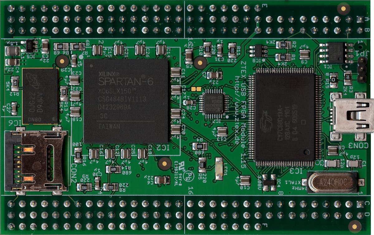
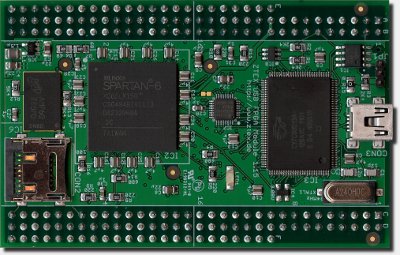
USB-FPGA Module 1.15d with Spartan 6 LX150 (XC6SLX150). Also available with LX45 (1.15a, XC6SLX45), LX75 (1.15b, XC6SLX75) and LX100 (1.15d, XC6SLX100) |
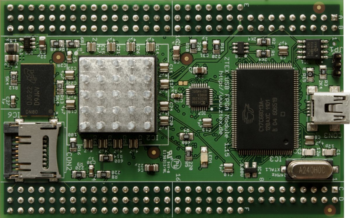
USB-FPGA Module 1.15 with 18×18mm heat sink. These heat sinks are delivered with the LX45 (1.15a, XC6SLX45) and LX75 (1.15b XC6SLX75) variants of the FPGA Board. |
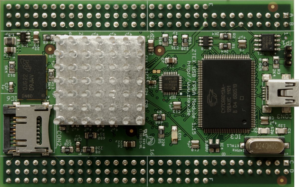
USB-FPGA Module 1.15 with 25×25mm heat sink. These heat sinks are delivered with the LX100 (1.15c, XC6SLX100) and LX150 (1.15d, XC6SLX150) variants of the FPGA Board. |

Size comparison of the Spartan 6 USB-FPGA Module 1.15. These FPGA Boards are available in four variants: 1.15a (LX45 / XC6SLX45), 1.15b (LX75 / XC6SLX75), 1.15c (LX100 / XC6SLX100) und 1.15d (LX150 / XC6SLX150). |