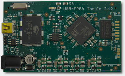
USB-FPGA Module 2.12:
FPGA Board with Artix 7, EZ-USB FX2 and DDR3 SDRAM
|
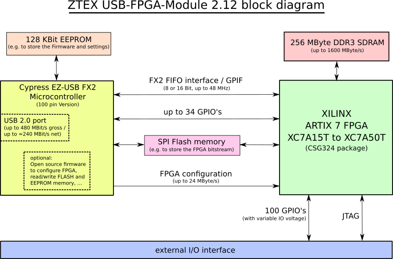
Block diagram
Schematics (PDF) |
 |
Block diagram
Features
- USB 2.0 interface with Mini-USB connector (B-type)
- Cypress CY7C68013A EZ-USB FX2 Microcontroller (100 pin version)
- Three possible Xilinx Artix 7 FPGA variants: XC7A15T, XC7A35T and XC7A50T, see Variants
- External I/O connector (consisting in two female 2x32 pin headers with 2.54mm grid) provides:
- 100 General Purpose I/O's (GPIO) connected to FPGA
- JTAG signals
- Reset signal
- External power (4.5 V .. 16 V) input
- 3.3V output
- I/O voltage output or input, see External I/O connector
- Same pin assignment as USB-FPGA Module 2.14 and USB-FPGA Module 2.13
-
256 MByte DDR3 SDRAM:
- Up to 400 MHz clock frequency
- 16 Bit bus width
- Up to 1600 MByte/s data rate
- Usable with the Xilinx Memory Interface Generator (MIG), examples are included in the SDK
- 128 MBit on-board Flash memory
- Allows Bitstream loading from Flash to FPGA (up to 16.5 MByte/s)
- Accessible from EZ-USB FX2 and from FPGA, but not while the EZ-USB FX2 GPIF/FIFO interface is in use
- Unique non-erasable ID which can be used to generate a serial number
- 128 Kbit EEPROM memory (can be used to store the EZ-USB firmware and board settings)
- Fast FPGA configuration via USB: up to 24 MByte/s
- On-Board power supply:
- 3.3 V: 2000 mA
- 1.8 V: 2000 mA
- 1.5 V: 2000 mA
- 1.0 V: 2000 mA
- Optional:
- Battery to store a key for bitstream encryption
- On-board JTAG connector
Compatibility with USB-FPGA Modules 2.13
USB-FPGA Modules 2.12 are a modified version of USB-FPGA Modules 2.13. They where developed in response to component shortage and will replace the smaller variants of USB-FPGA Modules 2.13. Besides of the different voltage regulators there are a few incompatibilities:
| Change | Porting recommendation |
Signals connected to PC7 and PB0 of EZ-USB FX2 are swapped. Flash DIN is now at at PB0. |
Swap FPGA balls K17 ⟷ M16 in the constraint file |
Signals connected to PC4 and PB1 of EZ-USB FX2 are swapped. Flash DOUT is now at at PB1. |
Swap FPGA balls K18 ⟷ L16 in the constraint file |
| No MAC-EEPROM | Unique non-erasable device ID (which is used to generate the serial number by default) is now read form the Flash. Configuration data is stored in last sector of firmware EEPROM. These changes are automatically considered by the new firmware. |
| Flash and FX2 GPIF/FIFO interface can't be used at the same time |
In summary, instruction for porting from USB-FPGA Modules 2.13 are:
- Custom firmware has to be re-compiled for the new target (replace "
IDENTITY_UFM_2_13(10.17.0.0,0);" with "IDENTITY_UFM_2_12(10.43.0.0,0);") If you use the default firmware, just use the new (pre-installed) default firmware. - In the constraint file of your FPGA project: Swap FPGA balls
K17 ⟷ M16andK18 ⟷ L16and rebuild the bitstream. (If you do not use these pins, you can re-use the old bitstreams without modification.)
Variants
These variants with different FPGA's can be offered:
| Variant | FPGA | Speed grade (larger means faster) |
Temperature range | Availability |
| USB-FPGA Module 2.12a | XC7A15T | 1C | 0-70°C | Available on-request. (Minimum order quantity >100. Long lead time.) |
| USB-FPGA Module 2.12b | XC7A35T | 1C | 0-70°C | In production. Replacement for USB-FPGA Module 2.13a. to the Shop |
| USB-FPGA Module 2.12c | XC7A50T | ? | ? | Possible replacement for USB-FPGA Module 2.13b(2) in future. |
All variants are supported by the free Vivado Webpack versions.
Functional description
The following drawing shows the measurements and the location of the described elements.
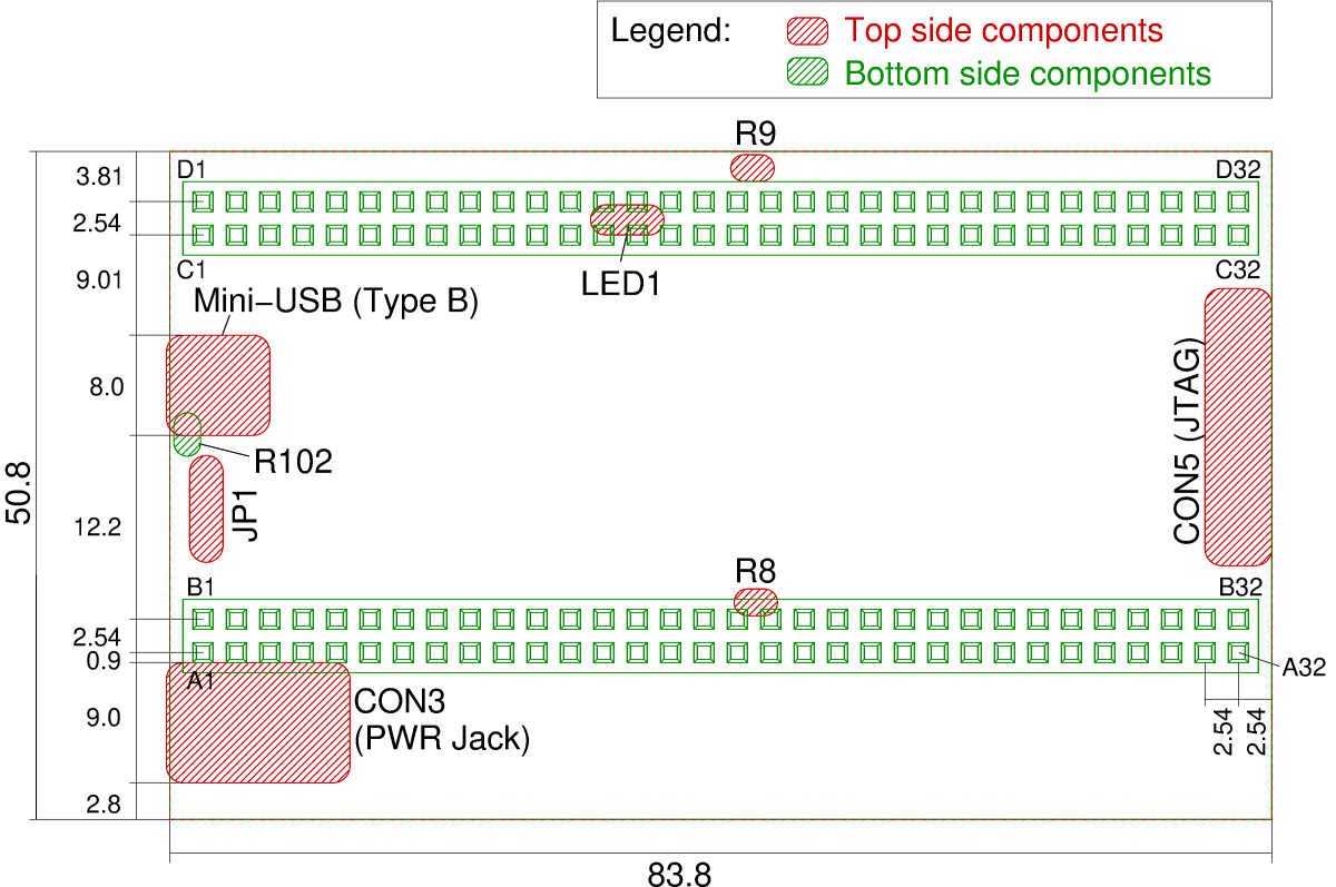
Click on the image for a larger version or download the PDF version.
USB-FPGA Modules 2.12 have no mounting holes because they are usually plugged onto an application circuit. Alternatively also one of the add-on cards may be used as mounting adapter.
Common functions of all Series 2 FPGA Boards
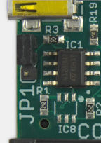
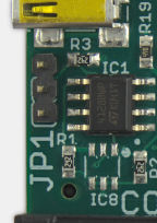
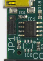
USB-FPGA Modules 2.12 belong to ZTEX FPGA Board Series 2. All functions that are shared with the other members of this Series are described on the Series 2 FPGA Board pageEEPROM address: JP1
Jumper JP1 specifies the I2C address of the EEPROM:
| JP1 | I2C address |
| open | 0xA2 |
| close | 0xAA |
JP1 is used tp prevent Firmware booting from EEPROM, e.g. if the firmware is corrupt. At booting the EZ-USB FX2 Microcontroller expects the firmware at the I2C address 0xA2 (jumper open) and falls back to an internal firmware if no valid data is found at this address (jumper closed).
JP1 has an unconnected pin which can be used for parking the jumper. The following pictures show all possible jumper positions:
|
|
| JP1 open | JP1 closed |
FPGA state: LED1
LED1 indicates the configuration state of the FPGA as follows:
| LED1 | FPGA |
| on | unconfigured |
| off | configured |
Power connector: CON3
External power can be supplied via CON3 or pins A1 and B1 of the external I/O connector. CON3 is a standard DC power jack with 2.1mm center pin (+) diameter and 5.5mm barrel (-) diameter for a supply voltage of 4.5 V to 16 V. A1 and B1 of the I/O connector and the center pin of CON3 are connected directly. This allows to supply a base board from the FPGA board.For most applications (especially if memory if used) USB standard does not guaranty sufficient current in order to power USB-FPGA Modules 2.12. Nevertheless, the FPGA Board can be powered from USB if the optional 0 Ω resistor R102 (package 0805) is installed (bottom side below USB connector, see drawing). In that case care must be taken in order to prevent that no second power external power supply is connected to CON3 or pins A1 and B1 of the external I/O connector.
Clock resources
On the FPGA board two clocks sources are connected to the FPGA: the clock output of the EZ-USB FX2 which is usually configured to 48 MHz and the interface clock which can be configured to 30 MHz or to 48 MHz. They can be used to generate new clocks within the FPGA using MMCM's or PLL's.Additional clocks can be connect to the MRCC and SRCC pins of the I/O connector. (These pins are arranged as differential pairs, e.g. L12P_T1_MRCC_35 and L12N_T1_MRCC_35. Single ended clocks must be connected to the positive pin, e.g. L12P_T1_MRCC_35.)
In most cases the on board clock sources are sufficient.
FPGA Configuration
The FPGA can be configured via USB, from Flash or via JTAG. Configuration via USB is either possible using EP0 transfer (slow, always available) or using a hi-speed endpoint (up to 24 MByte/s) which can be re-used after FPGA configuration. The default firmware supports both modes.More information about using the Flash for FPGA configuration can be found on the ZTEX Wiki.
I/O Connector
The external I/O connector is compatible to other FPGA Boards of the Series 2 and therefore described at page of Series 2 FPGA Boards. The pin assignment is the same as for USB-FPGA Modules 2.14. This allows easy migration between these two FPGA-Boards.On USB-FPGA Modules 2.12 all 100 external I/O's are assigned and have a variable I/O voltage. I/O voltage for rows A and B is VCCO_AB and for rows C and D it is VCCO_CD. By default VCCO_AB and VCCO_CD are connected to 3.3V through 0Ω resistors R8 and R9, respectively. Thus, these pins are 3.3V outputs. (This is the standard behaviour for all FPGA Boards of the Series 2.) If another I/O voltage is required, R8 and/or R9 can be unsoldered and VCCO_AB and/or VCCO_CD can be used as voltage input.
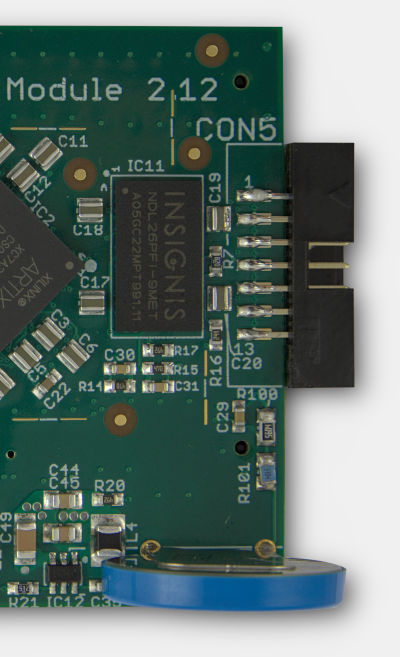
JTAGThe FPGA can be configured either via USB or via JTAG. JTAG signals are available on the external I/O connector and JTAG headers are installed on most add-on cards. Optionally a 14 pin header (CON5) can be installed as depicted on the side. (By default it is not installed for space reasons). The JTAG headers are available in the shop. Battery optionIf Bitstream encryption is required a standard 3V Lithium battery with a pin distance of 10×3mm can be installed. Furthermore two 0805 SMD resistors need to be soldered, R100: 5.6 MΩ and R101: 3.3 MΩ. Taking into account the battery degeneration the data retention time should be at least 10 years.The battery allows the FPGA to store a key which is used for bitstream encryption in a special low-power memory. The key has to be uploaded via JTAG. In order to prevent damage R100 must be soldered before the battery is installed. Also care should be taken in order to prevent shortcuts that can cause voltage drop and loss of encryption data. The picture on the side shows an USB-FPGA Module 2.12 with installed battery, R100, R101 and JTAG header CON5. FPGA Boards with factory-installed battery components and/or JTAG are available on request. Instructions for Bitstream encryption can be found on the Wiki. |
 |
Images
Click on the images for larger versions.
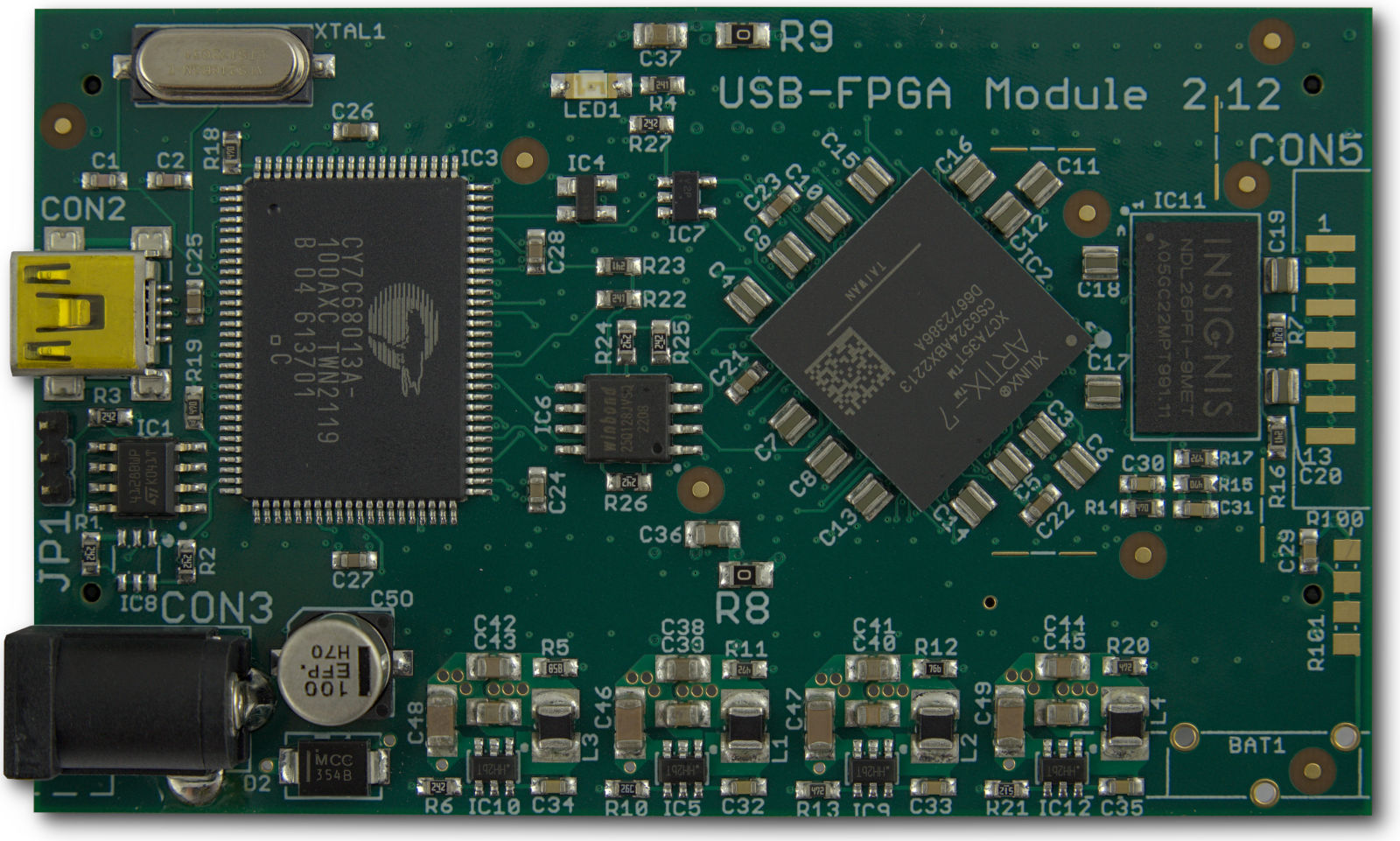
Top side of USB-FPGA Module 2.12b with Artix 7 FPGA XC7A35T. |
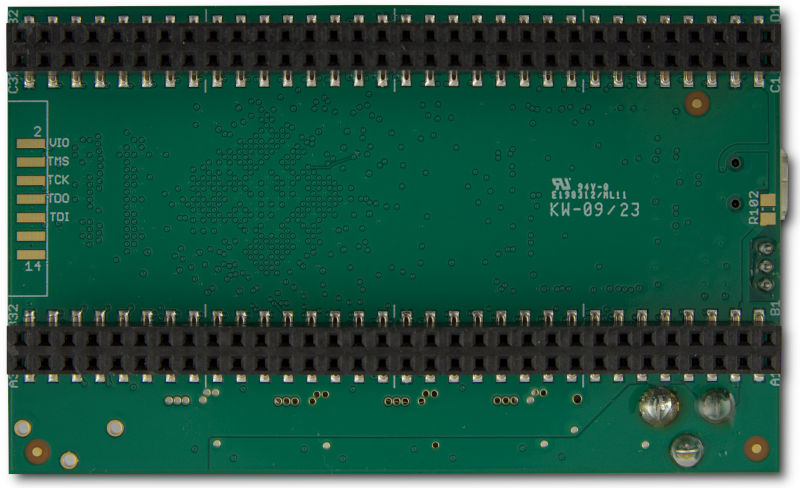
Bottom side of USB-FPGA Module 2.12. |