USB-FPGA Module 1.2:
Spartan 3 FPGA Board with USB 2.0 Microcontroller
USB-FPGA Modules 1.2 are deprecated. Please switch to Series 2 FPGA Boards.
An Adapter is available as workaround.
The old product page is still available here for documentation purposes.
|
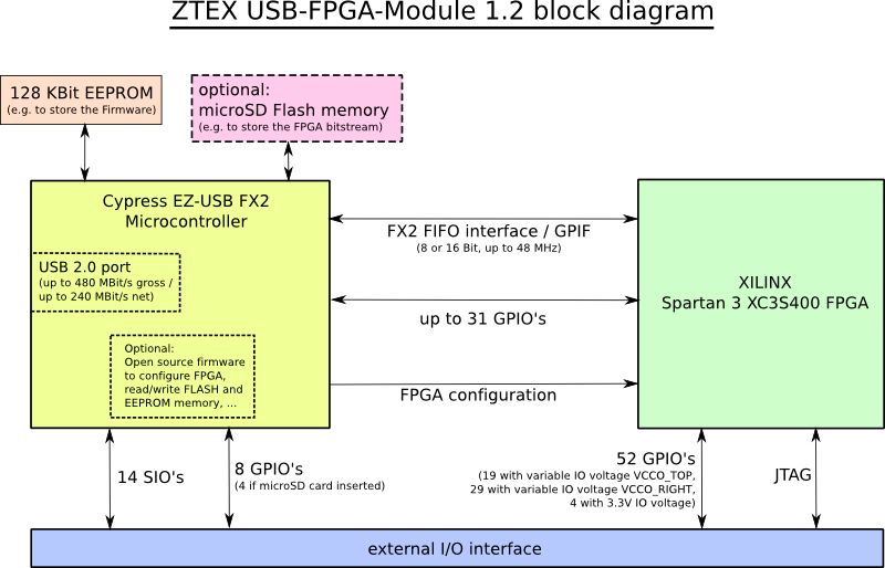
Block diagram
Schematics (PDF) |
 |
Block diagram
Features
- High-Speed (480 MBit/s) USB interface via Mini-USB connector (B-type)
- Cypress CY7C68013A/14A EZ-USB FX2 Microcontroller
- Xilinx Spartan-3 XC3S400 FPGA
-
60 General Purpose I/O's (GPIO):
- 52 FPGA GPIO's
- 8 EZ-USB FX2 GPIO's (4 if Flash option is installed)
-
20 special I/O's (SIO):
- 6 SIO's for FPGA configuration including JTAG
- 2 serial ports (4 pins)
- I2C interface (2 pins)
- 2 interrupts
- 3 timers
- 1 clock output
- 1 Wakeup pin
- 1 Breakpoint pin
- External power supply required:
- 3.3 V; supply current depends on application (see XC3S400 datasheet), recommended: ≥ 500 mA
- 2.5 V; supply current depends on application (see XC3S400 datasheet), recommended: ≥ 200 mA
- 1.2 V; supply current depends on application (see XC3S400 datasheet), recommended: ≥ 500 mA
- Variable I/O voltage VCCO_RIGHT: 1.14...3.46 V; supply current depends on application (see XC3S400 datasheet), recommended: ≥ 500 mA
- Variable I/O voltage VCCO_TOP: 1.14...3.46 V; supply current depends on application (see XC3S400 datasheet), recommended: ≥ 500 mA
- FPGA configuration / programming via USB using the EZ-USB FX2 SDK. (No JTAG adapters or other additional utilities required.)
- 128 Kbit EEPROM memory (can be used to store the EZ-USB firmware)
- Flash memory (optionally)
SDK, Examples, Getting Started
A powerful open source Firmware Development Kit with platform independent host software API is available for the USB-FPGA Board. This SDK allows to define all USB device descriptors using only a few macro commands, and thus gives the developer a quick start into Firmware programming.The SDK package contains a lot of examples which can be used as starting point for own applications.
More Information are available in the EZ-USB FX2 SDK section.
Additional documentation including Tutorials can also be found on the ZTEX Wiki
Functional description
The following drawing shows the measurements and the location of the of the described elements.
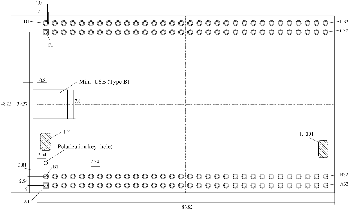
Click on the image for a larger version or download the PDF version.
EEPROM address: JP1
Jumper JP1 specifies the I2C address of the EEPROM:
| JP1 | I2C address |
| open | 0xA2 |
| close | 0xAA |
The EZ-USB FX2 Microcontroller searches for the firmware at the address 0xA2 which is the default address (jumper open).
The main purpose of this jumper is to disable EEPROM boot-loading. If, for example, the EEPROM was programmed with a corrupt firmware the Microcontroller can be booted with the internal default firmware by short cutting the two pads of jumper JP1 during powering-on the USB-FPGA Module.
FPGA state: LED1
LED1 indicates the configuration state of the FPGA as follows:
| LED1 | FPGA |
| on | unconfigured |
| off | configured |
Flash options
There are two options to install additional Flash memory on USB-FPGA Modules 1.2. Both options are soldered on the bottom side of the module and are connected to pins PE4 to PE7 of Port E of the EZ-USB FX2, see the circuit diagram.
Only one Flash option can be installed at a time.
Flash option 1
- Consists in R8 (51kΩ resistor, SMD 1206 package) and IC5 (AT45D* compatible Flash IC, SOIC8 package), see circuit diagram.
- Occupies pins C9 to C12 of the I/O connector, i.e. these pins are not available for application use.
- High reliability (20 years data retention).
- Currently not supported by the EZ-USB FX2 SDK.
- Installation hint: Pin 1 of IC5 is marked by a "1" in in the copper layer.
Flash option 2
- Consists in CON4 (Molex 500901-0801 compatible microSD socket), see circuit diagram.
- Does not permanently occupy pins C9 to C12 of the I/O connector (pins PE4 to PE7 of the EZ-USB FX2), i.e. if no card is inserted, these pins are available for application use.
- Support of standard and high capacity (SDHC) cards
- Supported by the EZ-USB FX2 SDK (the cards must support the SPI mode).
I/O Connector
Two 2x32 pin connectors deliver the I/O signals and are used for the power supply. The drawing shows the position of these connectors.
The I/O connector of the USB-FPGA Module 1.2 is mechanical upward compatible to the I/O Connector of the Spartan 6 USB-FPGA Module 1.11.
There is a polarization key in form of a small hole close to the B1 pin as shown on the drawing. In order to prevent damage equal orientation of the polarization key (hole) of all stacked boards must be ensured.
JTAG
The I/O connector contains 4 JTAG signals. If the JTAG interface is used for FPGA configuration bit 1 of port A (=PROG_B at FPGA) must be driven high. This happens automatically if a firmware developed with the SDK is running.
Pinlist and List of Connections
The Pinlist of the I/O Connector and the List of Connections can be downloaded in Gnumeric or Excel format. These files contain the data for all USB-FPGA Boards including compatibility information. (Attention: The files contain several sheets.)
This is the Pinlist of the I/O Connector:
| Pinlist | ||||||
| A | B | C | D | |||
| 1 | 5..15V | 5..15V | USB_5V | USB_5V | 1 | |
| 2 | GND | GND | 5V (unused) | 5V (unused) | 2 | |
| 3 | INT4 | T0 | CLKOUT | 5V (unused) | 3 | |
| 4 | T1 | T2 | GND | GND | 4 | |
| 5 | BKPT | GND | INT5# | WAKEUP* | 5 | |
| 6 | SCL | SDA | 3.3V | 3.3V | 6 | |
| 7 | 3.3V | 3.3V | VCCO_TOP | VCCO_TOP | 7 | |
| 8 | TxD0 | RxD0 | GND | 5~L20P_7 | 8 | |
| 9 | TxD1 | RxD1 | PE7 | 4~IO/VREF_7 | 9 | |
| 10 | 2.5V | 2.5V | PE6 | 2~IO_L01N_7/VRP_7 | 10 | |
| 11 | 1.2V | 1.2V | PE5 | 1~IO_L01P_7/VRN_7 | 11 | |
| 12 | 74~IO_L01N_3/VRP_3 | 73~IO_L01P_3/VRN_3 | PE4 | 141~IO_L01N_0/VRP_0 | 12 | |
| 13 | 76~IO | GND | PE3 | 140~IO_L01P_0/VRN_0 | 13 | |
| 14 | 78~IO_L20N_3 | 77~IO_L20P_3 | PE2 | 137~IO_L27N_0 | 14 | |
| 15 | 80~IO_L21N_3 | 79~IO_L21P_3 | PE1 | 135~IO_L27P_0 | 15 | |
| 16 | 3.3V | 3.3V | PE0 | 132~IO_L30N_0 | 16 | |
| 17 | 83~IO_L22N_3 | 82~IO_L22P_3 | GND | 131~IO_L30P_0 | 17 | |
| 18 | 85~IO_L23N_3 | 84~IO_L23P_3/VREF_3 | 2.5V | 2.5V | 18 | |
| 19 | 87~IO_L24N_3 | 86~IO_L24P_3 | 1.2V | 130~IO_L31N_0 | 19 | |
| 20 | 90~IO_L40N_3/VREF_3 | 89~IO_L40P_3 | 128~IO_L32N_0/GCLK7 | 129~IO_L31P_0/VREF_0 | 20 | |
| 21 | GND | GND | 125~IO_L32N_1/GCLK5 | 127~IO_L32P_0/GCKL6 | 21 | |
| 22 | VCCO_RIGHT | VCCO_RIGHT | 123~IO_L31N_1/VREF_1 | 124~IO_L32P_1/GCLK4 | 22 | |
| 23 | 1.2V | 1.2V | 119~IO_L28N_1 | 122~IO_L31P_1 | 23 | |
| 24 | 93~IO_L40N_2 | 92~IO_L40P_2/VREF_2 | 116~IO | 118~IO_L28P_1 | 24 | |
| 25 | 96~IO_L24N_2 | 95~IO_L24P_2 | 112~IO_L01P_1/VRN_1 | 113~IO_L01N_1/VRP_1 | 25 | |
| 26 | 98~IO_L23N_2/VREF_2 | 97~IO_L23P_2 | GND | GND | 26 | |
| 27 | 100~IO_L22N_2 | 99~IO_L22P_2 | VCCO_TOP | VCCO_TOP | 27 | |
| 28 | 103~IO_L21N_2 | 102~IO_L21P_2 | 1.2V | 1.2V | 28 | |
| 29 | 105~IO_L20N_2 | 104~IO_L20P_2 | 2.5V | TDI | 29 | |
| 30 | 108~IO_L01N_2/VRP_2 | 107~IO_L01P_2/VRP_2 | M0 | TMS | 30 | |
| 31 | VCCO_RIGHT | VCCO_RIGHT | M1 | TCK | 31 | |
| 32 | GND | GND | GND | TDO | 32 | |
| Summary | ||||
| A/B | C/D | |||
| FPGA-IO | 29 | FPGA-IO | 23 | |
| Serial | 4 | FX2-IO | 8 | |
| I2C | 2 | CLK | 1 | |
| Timer | 3 | Interrupt | 1 | |
| Interrupt | 1 | Wakeup | 1 | |
| Breakpoint | 1 | JTAG | 6 | |
| 3.3V | 4 | 3.3V | 2 | |
| VCCO_RIGHT | 4 | VCCO_TOP | 4 | |
| 2.5V | 2 | 2.5V | 3 | |
| 1.2V | 4 | 1.2V | 3 | |
| 5..15V | 2 | 5V | 3 | |
| GND | 8 | USB 5V | 2 | |
| GND | 7 | |||
| FPGA-GPIO | 29 | FPGA-GPIO | 23 | |
| SIO (special I/O) | 11 | FX2-GPIO | 8 | |
| Power | 24 | SIO (special I/O) | 9 | |
| Sum | 64 | Power | 24 | |
| Sum | 64 | |||
Images
Click on the images for larger versions.
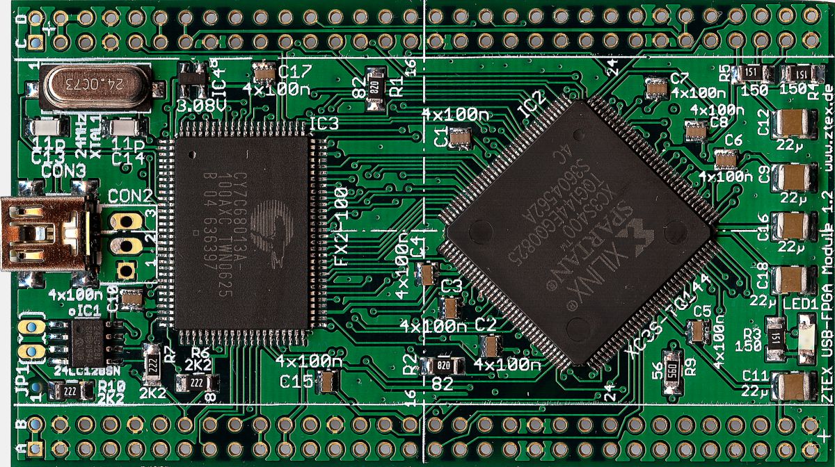
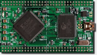
Top side of the USB-FPGA Module 1.2. |
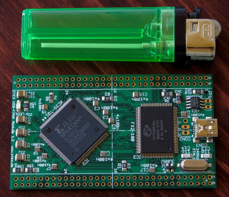
Size comparison of the USB-FPGA Module 1.2. |