FPGA Module 2.00: Spartan 6 FPGA Board
|
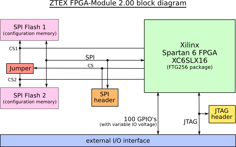
Block diagram
Schematics (PDF) |
 |
Block diagram
Features
- Xilinx Spartan 6 XC6SLX16 FPGA (XC6SLX9 and XC6SLX25 on request)
- External I/O connector (consisting in two female 2x32 pin headers with 2.54mm grid) provides:
- 100 General Purpose I/O's (GPIO) connected to FPGA
- JTAG signals
- Reset signal
- External power (4.5 V .. 16 V) input
- 3.3V output
- I/O voltage output or input, see External I/O connector
- Dual 16 MBit on-board Flash
- Can be used for FPGA configuration from Flash (up to 6.5 MByte/s)
- Chip selectable by jumper
- On-Board power supply:
- Power inputs: USB connector or External I/O connector
- 3.3 V: 2000 mA
- 1.2 V; 1000 mA
- Temperature range: 0-70°C
Variants
Three variants with different FPGA's are offered:
| Variant | FPGA | Speed grade (larger means faster) |
Availability |
| FPGA Module 2.00a | XC6SLX16 | 2 | On request (no stock type) |
| FPGA Module 2.00b | XC6SLX16 | 2 | Stock type, to the shop |
| FPGA Module 2.00c | XC6SLX25 | 3 | On request (no stock type) |
All variants are supported by the free ISE Webpack versions.
Examples and Templates
USB-FPGA Modules 2.00 ares not supported by the ZTEX SDK because it has no PC-Interface (other than JAG). Instead of this there is an example package which also includes constraints templates. It's available in .tar.bz2 and .zip format.Functional description
The following drawing shows the measurements and the location of the components described here.
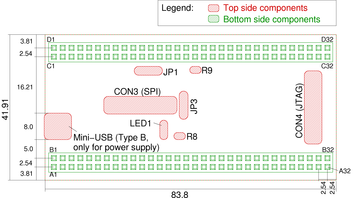
Click on the image for a larger version or download the PDF version.
FPGA Modules 2.00 have no mounting holes because they are usually plugged onto an application circuit. Alternatively also one of the add-on cards may be used as mounting adapter.
FPGA configuration
There are two ways to configure the FPGA:- Via JTAG, see JTAG section below.
- From Flash, see Flash section below.
Powering
External power can be supplied via a Mini USB connector (which can only be used for powering) or pins A1 and B1 of the external I/O connector. Powering through thr USB connector can be disabled by removing 0 Ω resistor R10. This is desirable in order to prevent damage caused by accidental connection of an USB cable if the FPGA Board is powered from the External I/O connector.Reset, JP1
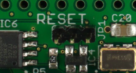
FPGA Modules 2.00 have a reset circuit. Reset can be asserted by:- Pulling low pin D1 of external I/O connector
- Closing Jumper JP1
- Pulling low pin T4 of the FPGA
Important: The bitstream must ensure that pin T4 of the FPGA is either floating or pulled high, see the examples.
JP1 has an unconnected pin which can be used for parking the jumper. The following pictures show all possible jumper positions:
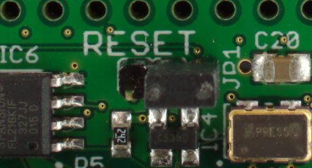
|
JP1 open |
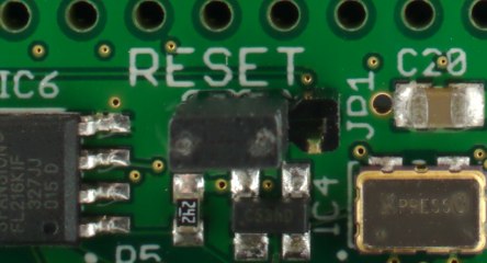
|
JP1 closed |
FPGA state: LED1
LED1 indicates the configuration state of the FPGA as follows:
| LED1 | FPGA |
| on | unconfigured |
| off | configured |
Clock resources
FPGA Modules 2.00 have a 26 MHz oscillator which is connected to pin T7 of the FPGA. This clock can be used to generate new clocks within the FPGA using DCM's or PLL's.Additional clocks can be connect to the GCLK pins of the I/O connector.
Flash, JP3
FPGA Modules 2.00 have two 16 MBit SPI Flash memory chips. In most cases they are used for FPGA configuration.Both Flash ICs are connected to a common SPI bus but there are three chip select (CS) signals. CS1# is connected directly to Flash 1 (IC6) and CS2# is connected to Flash 2 (IC1), see schematics. CS# is switched through JP3 either to Flash 1 or to Flash 2. Thus, if the Flash is used for FPGA configuration, the bitstream source is selected by JP3:
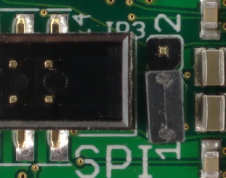
|
Flash 1 selected |
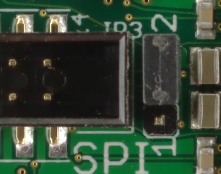
|
Flash 2 selected |
The maximum configuration speed is 6.5 Mbyte/s and is achieved at 26 MHz SPI Bus speed and 2 Bit SPI Bus width (bitgen settings -g ConfigRate:26 -g SPI_buswidth:2). Bitstream can be written to the Flash using the indirect programming method of the Xilinx Tools (see ZTEX Wiki) or through the SPI header CON3 with the following standard pin assignment:
| Signal | Pins | Notes |
| MOSI | 10 | = Flash DIN |
| MISO | 8 | = Flash DOUT |
| SS | 4 | CS# signal, selects Flash 1 or 2 depending on position of JP3 |
| SCK | 6 | = Flash CLK |
| WP | 14 | pulled high on board |
| VIO | 2 | 3.3 V |
| GND | 1,3,5,7,9,11,13 |
I/O Connector
The external I/O connector is compatible to other FPGA Boards of the Series 2 and therefore described at page of Series 2 FPGA Boards.On FPGA Modules 2.00 all 100 external I/O's are assigned and have a variable I/O voltage. I/O voltage for rows A and B is VCCO_AB and for rows C and D it is VCCO_CD. By default VCCO_AB and VCCO_CD are connected to 3.3V through 0Ω resistors R8 and R9, respectively. Thus, these pins are 3.3V outputs. (This is the standard behaviour for all FPGA Boards of the Series 2.) If another I/O voltage is required, R8 and/or R9 can be unsoldered and VCCO_AB and/or VCCO_CD can be used as voltage input.
FPGA Modules 2.00 have dual entry female pin headers, i.e. user circuits can be connected to both sides. Plugging user PCB's to top side (component side) of the FPGA Board requires non-standard pin headers with long pins. (The pin headers headers which ara available in the Shop can only be used to connect circuits to bottom side).
The pin assignment of FPGA Modules 2.00 and USB-FPGA Modules 2.01 are equal.
JTAG
JTAG signals are available on the on-board JTAG header CON4 and external I/O connector. CON4 has standard pin assignment:
| Signal | Pins | Notes |
| TDI | 10 | |
| TDO | 8 | |
| TMS | 4 | |
| TCK | 6 | |
| VIO | 2 | 3.3 V |
| GND | 1,3,5,7,9,11,13 |
Images
Click on the images for larger versions.
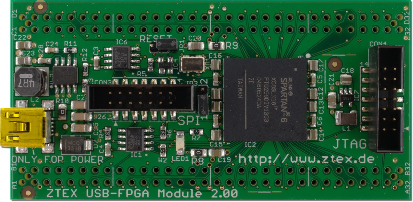
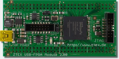
Top side of FPGA Module 2.00b with Spartan 6 XC6SLX16 FPGA. |
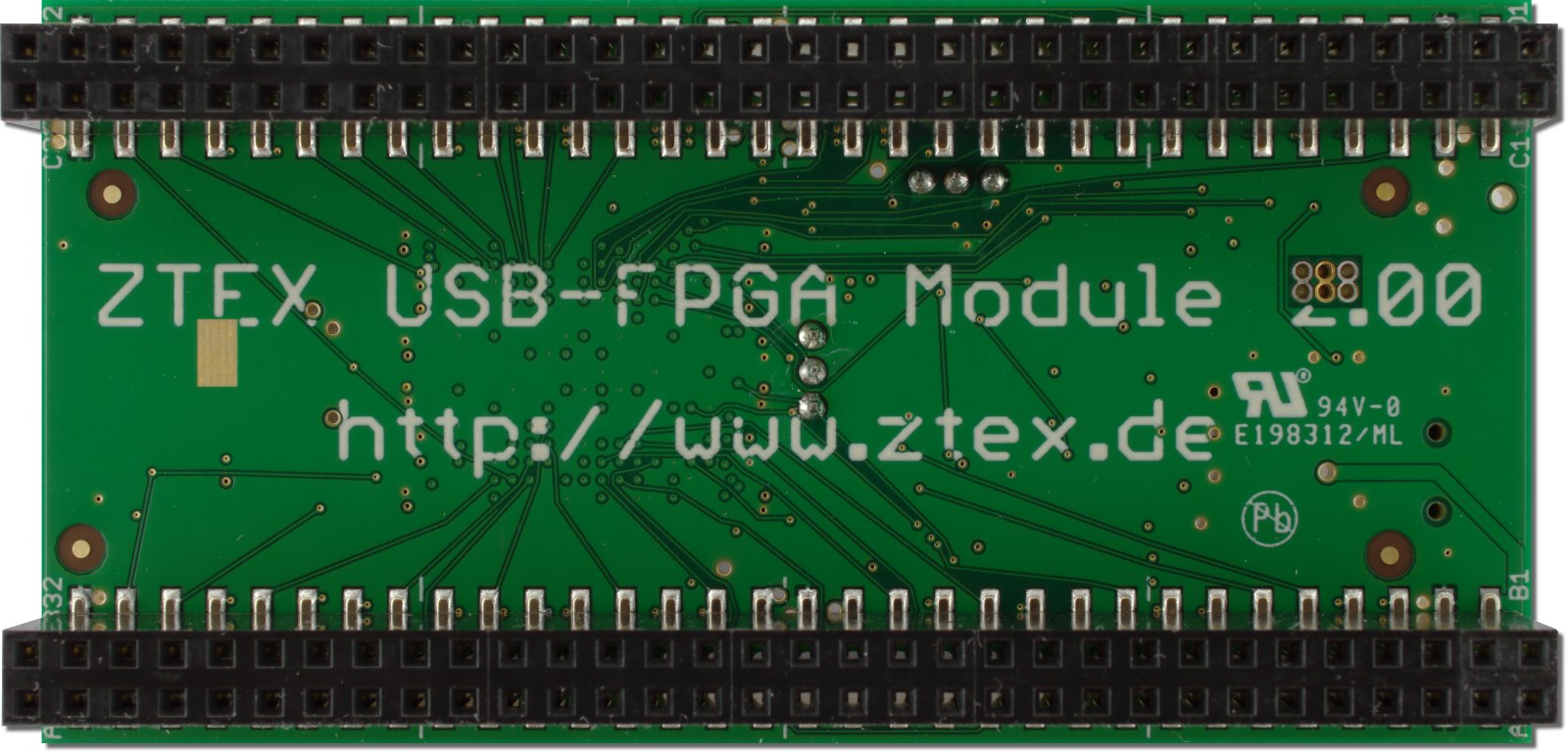
Bottom side of FPGA Module 2.00b. |