USB-FPGA Module 2.16:
FPGA Board with Artix 7 XC7A200T and EZ-USB FX2.
|
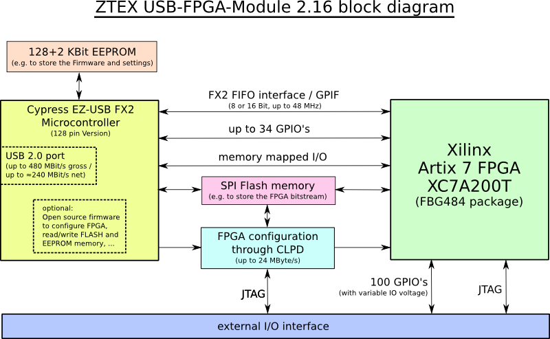
Block diagram
Schematics (PDF) |
 |
Block diagram
Features
- High-Speed (480 MBit/s) USB interface via Mini-USB connector (B-type)
- Cypress CY7C68013A EZ-USB FX2 Microcontroller (128 pin version)
- Two Xilinx Artix 7 FPGA variants: XC7A200T (stock type) and XC7A100T (on request), see Variants
- External I/O connector (consisting in two female 2x32 pin headers with 2.54mm grid) provides:
- 100 General Purpose I/O's (GPIO) connected to FPGA
- JTAG signals
- Reset signal
- External power (4,5 V .. 16 V) input
- 3.3V output
- I/O voltage output or input, see External I/O connector
- 128 MBit on-board Flash memory
- Allows Bitstream loading from Flash to FPGA (up to 16.5 MByte/s)
- Accessible from EZ-USB FX2 and from FPGA, see the CPLD description
- Fast FPGA configuration via USB using CPLD: up to 24 MByte/s
- Memory mapped IO between EZ-USB FX2 and FPGA
- 128 Kbit EEPROM memory (can be used to store the EZ-USB firmware)
- 2 Kbit MAC-EEPROM: contains a unique non erasable MAC-address and is used to store firmware settings
- On-Board power supply:
- 3.3 V: 2000 mA
- 1.8 V: 1000 mA
- 1.0 V: 14000 mA
- Heat sink for high performance / high speed applications, see Section heat sink
- Optional:
- Battery to store a key for bitstream encryption
- On-board JTAG connector
- Temperature range: Board: 0-70°C; max. FPGA temperature see below
Variants
Variants with different features are offered:
| Variant | FPGA | Speed grade (larger means faster) |
FPGA temperature | Availability |
| USB-FPGA Module 2.16a | XC7A100T | 2C | 0-85°C | On request (no stock type) |
| USB-FPGA Module 2.16b | XC7A200T | 2C | 0-85°C | Stock type, to the Shop replaced by faster and fully compatible variant 2.16b2 |
| USB-FPGA Module 2.16b2 | XC7A200T | 3E | 0-100°C | Stock type, to the Shop long term availability |
All variants are supported by the free Vivado and ISE Webpack versions.
Functional description
The following drawing shows the measurements and the location of the of the described elements.
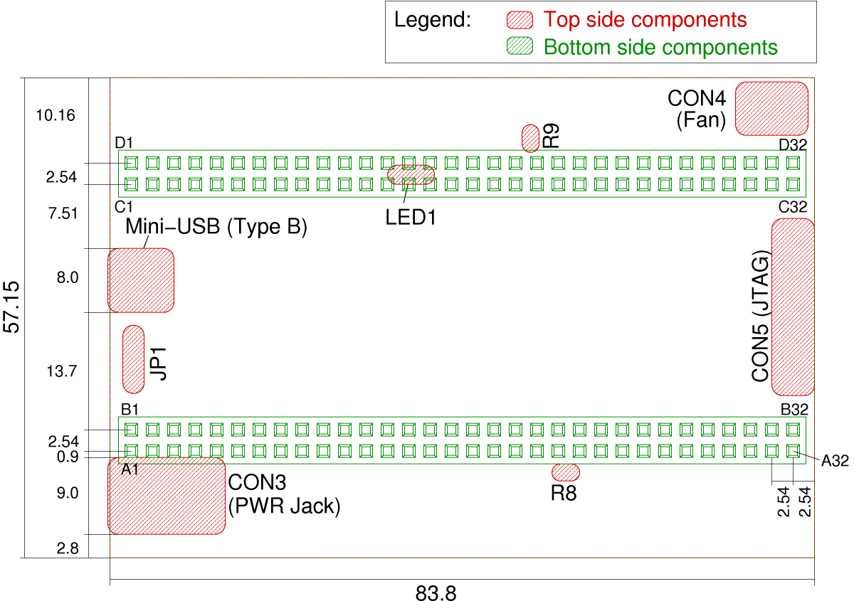
Click on the image for a larger version or download the PDF version.
The FPGA Board has no mounting holes because it is usually plugged onto an application circuit. If this is not present, e.g. if the FPGA board is used standalone as co-processor card, one of the add-on cards may be used as mounting adapter.
Common functions of all Series 2 FPGA Boards
USB-FPGA Modules 2.16 belong to ZTEX FPGA Board Series 2. All functions that are shared with the other members of this Series are described on the Series 2 FPGA Board pageEEPROM address: JP1
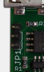
Jumper JP1 specifies the I2C address of the EEPROM:
| JP1 | I2C address |
| open | 0xA2 |
| close | 0xAA |
The EZ-USB FX2 Microcontroller searches for the firmware at the address 0xA2 which is the default address (jumper open).
The main purpose of this jumper is to suppress booting the Firmware from EEPROM. If, for example, the EEPROM was programmed with a corrupt firmware the Microcontroller can be booted with the internal firmware by closing JP1 during powering-on the FPGA Board.
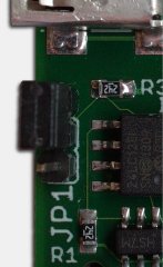
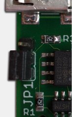
JP1 has an unconnected pin which can be used for parking the jumper. The following pictures show all possible jumper positions:
|
|
| JP1 open | JP1 closed |
FPGA state: LED1
LED1 indicates the configuration state of the FPGA as follows:
| LED1 | FPGA |
| on | unconfigured |
| off | configured |
Power connector: CON3
External power can be supplied via CON3 or pins A1 and B1 of the external I/O connector. CON3 is a standard DC power jack with 2.1mm center pin (+) diameter and 5.5mm barrel (-) diameter for a supply voltage of 4.5 V to 16 V. If a fan is installed to CON4 the input voltage should be 9V to 13V.A1 and B1 of the I/O connector and the center pin of CON3 are connected directly. This allows to supply a base board from the FPGA board.
Clock resources
On the FPGA board two clocks sources are connected to the FPGA: the clock output of the EZ-USB FX2 which is usually configured to 48 MHz and the interface clock which can be configured to 30 MHz or to 48 MHz. They can be used to generate new clocks within the FPGA using MMCM's or PLL's.Additional clocks can be connect to the MRCC and SRCC pins of the I/O connector. (These pins are arranged as differential pairs, e.g. L12P_T1_MRCC_35 and L12N_T1_MRCC_35. Single ended clocks must be connected to the positive pin, e.g. L12P_T1_MRCC_35.)
In most cases the on board clock sources are sufficient.
Configuration booster CPLD and Flash
The CPLD allows high speed configuration of the FPGA via USB (up to 24 MByte/s). This requires an output Endpoint of the EZ-USB FX2. The Firmware allows to (re-)use an endpoint which is intended for user defined communication. If all Endpoint buffers of the EZ-USB FX2 are required for input Endpoints standard speed (about 1 MByte/s) configuration via Endpoint 0 has to be used.The CPLD also controls the access of the Flash and FPGA configuration pins shared by different configuration sources. The following table gives an overview about the access and FPGA configuration modes. CM1:CM0 are the configuration mode pins of the CPLD and are driven by FX2. They are pulled up, i.e. default mode at FX2 start-up is 1:1. The mode pins M2:M1:M0 of the FPGA are driven by CPLD.
| CM1:CM0 | M2:M1:M0 | CCLK driven by: | Configuration source | Flash can be accessed by: |
| 1:1 | 1:0:1 | - | JTAG only | FX2 |
| 1:0 | 1:1:0 | FX2:CTL5 | USB (high speed mode, up to 24 MByte/s) or JTAG | - |
| 0:1 | 1:1:0 | FX2:PC6 | USB (low speed mode, about 1 MByte/s) or JTAG | - |
| 0:0 | 0:0:1 | FPGA | Flash (up to 16.5 MByte/s) or JTAG | FPGA (and FX2 after successful configuration) |
This table is just a brief summary because all configuration related issues are automatically handled by the firmware and the factory programmed CPLD. Interested user are referred to the schematics and the CPLD data package usb-fpga-2.13-2.16-cpld.zip which contains the source files and the jed file for programming the CPLD via JTAG.
More information about using the Flash for FPGA configuration can be found on the ZTEX Wiki.
I/O Connector
The external I/O connector is compatible to other FPGA Boards of the Series 2 and therefore described at page of Series 2 FPGA Boards.On USB-FPGA Modules 2.16 all 100 external I/O's are assigned and have a variable I/O voltage. I/O voltage for rows A and B is VCCO_AB and for rows C and D it is VCCO_CD. By default VCCO_AB and VCCO_CD are connected to 3.3V through 0Ω resistors R8 and R9, respectively. Thus, these pins are 3.3V outputs. (This is the standard behaviour for all FPGA Boards of the Series 2.) If another I/O voltage is required, R8 and/or R9 can be unsoldered and VCCO_AB and/or VCCO_CD can be used as voltage input.
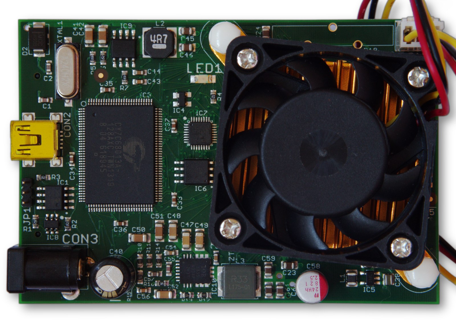
Heat sink, CON4
For high performance / high speed applications a heat sink is required. On USB-FPGA Modules 2.16 standard heat sinks with two push-pins with a distance of 59mm can be used.CON4 is a standard 3 pin fan connector for active coolers. If this connector is used the input voltage should be between 9V and 13V.
USB-FPGA Modules 2.16 are delivered with a cooler kit which consists in:
- 1 passive heat sink; height: 14mmm
- 1 active cooler; height with fan: 24mm
- 2 thermal pads with low thermal resistance
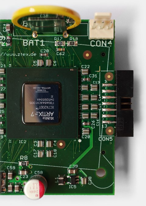
JTAGThe FPGA can be configured either via USB or via JTAG. JTAG signals are available on the external I/O connector and JTAG headers are installed on most add-on cards. Optionally a 14 pin header (CON5) can be installed as depicted on the side. (By default it is not installed for space reasons). The JTAG header is available in the shop. The JTAG interface can also be used for re-programming the CPLD. Battery optionIf Bitstream encryption is required a standard 3V Lithium battery with a pin distance of 10×3mm can be installed. Furthermore two 0805 SMD resistors need to be soldered, R17: 5.6 MΩ and R18: 3.3 MΩ. Taking into account the battery degeneration the data retention time should be at least 10 years.The battery allows the FPGA to store a key which is used for bitstream encryption in a special low-power memory. The key has to be uploaded via JTAG. In order to prevent damage R17 must be soldered before the battery is installed. Also care should be taken in order to prevent shortcuts that can cause voltage drop and loss of encryption data. The picture on the side shows an USB-FPGA Module 2.16 with installed battery, R17 and R18 and JTAG header CON5. FPGA Boards with factory-installed battery components and/or JTAG are available on request. Instructions for Bitstream encryption can be found on the Wiki. |
 |
Images
Click on the images for larger versions.
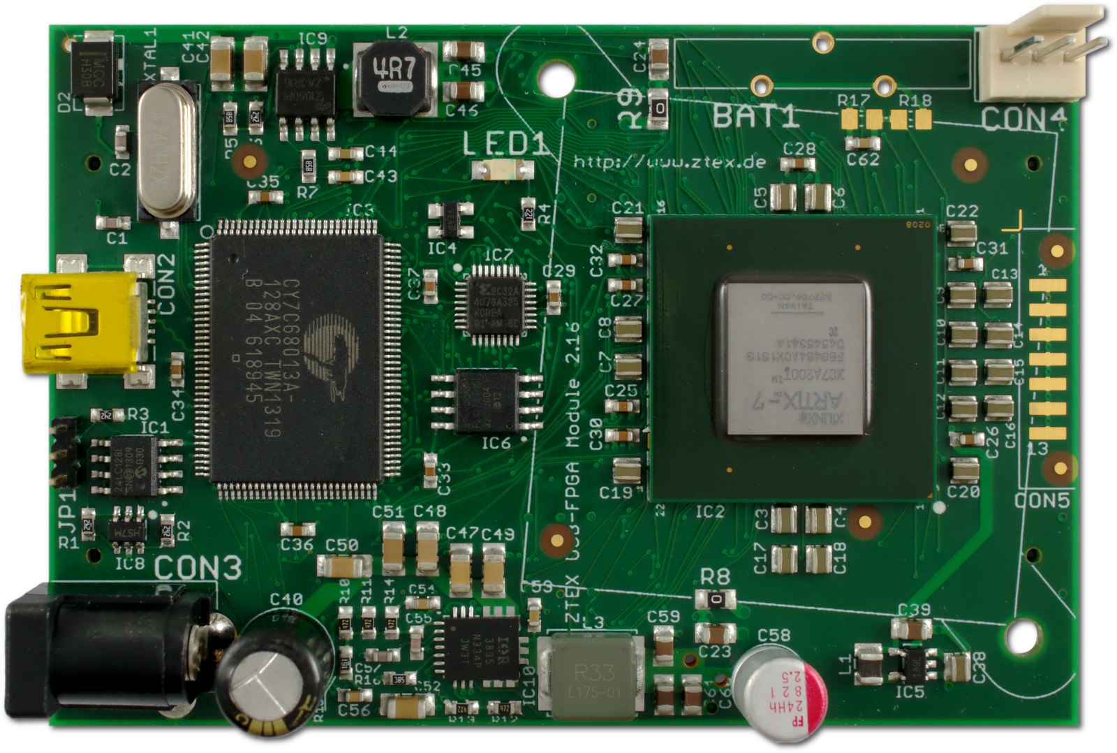
Top side of USB-FPGA Module 2.16b with Artix 7 FPGA XC7A200T. |
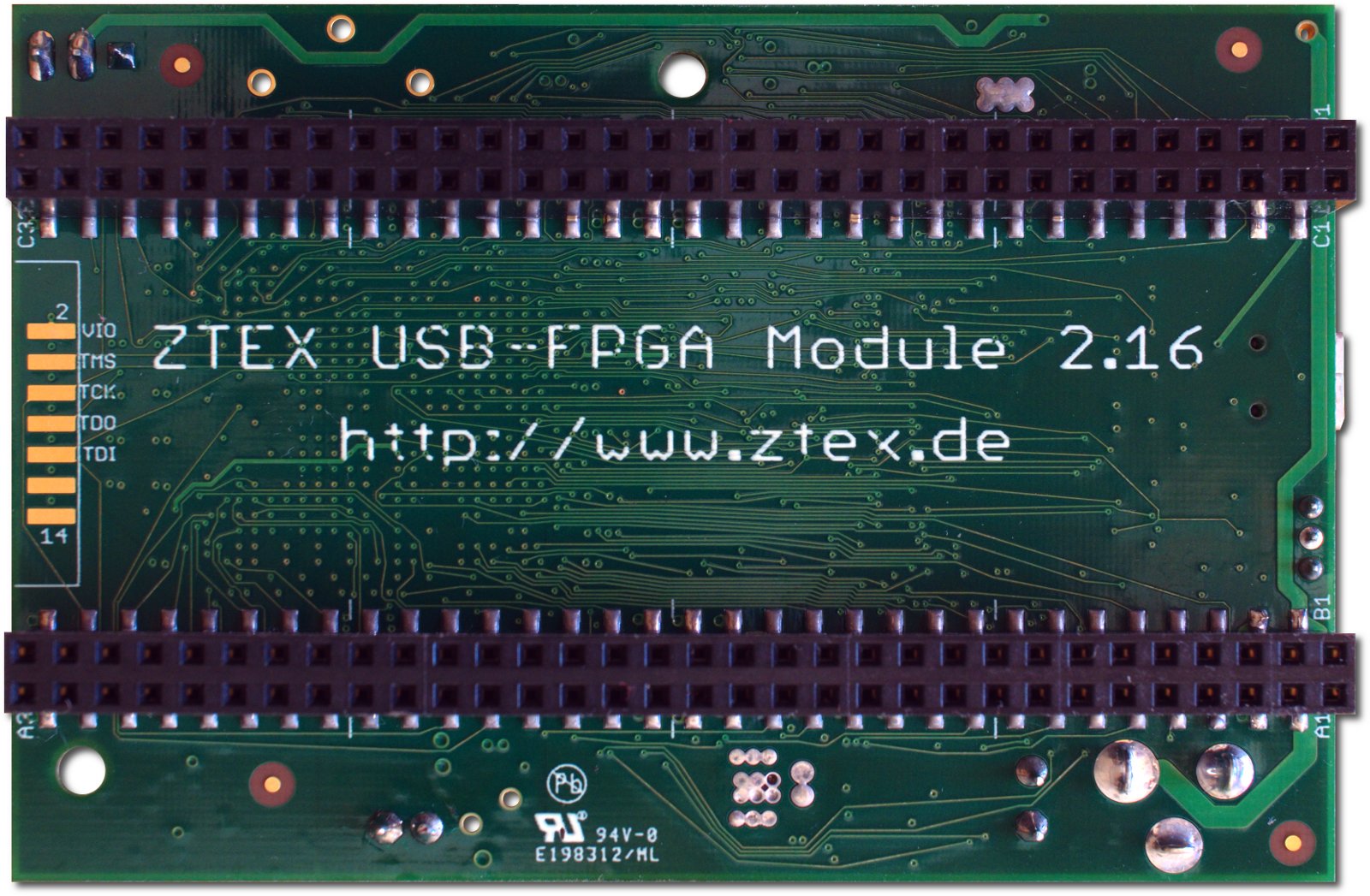
Bottom side of USB-FPGA Module 2.16 with Artix 7 FPGA. |
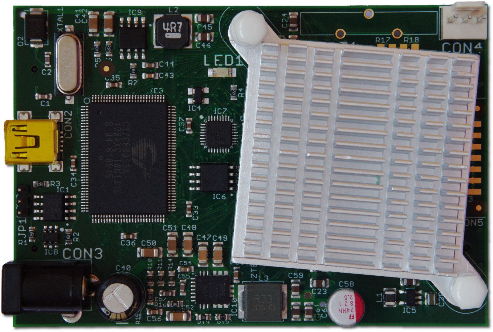
USB-FPGA Module 2.16 with passive (top) and active (bottom) cooler. Both heat sinks belong to the contents of delivery of the FPGA Board. |