Analog Experimental 1.10 Board for Series 1 FPGA Boards
Series 1 FPGA Boards are deprecated. Please switch to Series 2.
The old product page is still available here for documentation purposes.
|
Features Additional resources |
 |
Features
- Baseboard for USB-FPGA Modules 1.2 and 1.11
- High-efficiency switching regulators to generate the supply voltages
- 1.2 V @ 2.7 A
- 2.6 V @ 2.5 A
- 3.3 V @ 2.5 A
- Wide input range: 4.5 to 16 V
- AVR ATXmega128A1 microcontroller for analog capabilities:
- 2 eight-channel, 12 Bit, 2 Msps Analog to Digital Converter (ADC), software selectable gain of up to 64
- 2 two-channel, 12 Bit, 1 Msps Digital to Analog Converter (DAC)
- 4 Analog Comparators (AC) with Window-Function and input form DAC
- DMA controller for data transfers without CPU intervention
- Firmware programming and NVM access via USB using the EZ-USB FX2 SDK (no programming cables required)
- 128 KByte Flash + 2 KByte EEPROM
- Up to 76 General Purpose I/O's (GPIO's):
USB-FPGA Module 1.2 USB-FPGA Module 1.11 FPGA GPIO's (3.3 V) 31 49 XMEGA GPIO's (3.3 V) 27 27 Special I/O's 9 (I2C, two serial ports,
interrupts)6 (I2C, serial port,
interrupts) - I/O Ports available on a standard 2.54 mm (0.1 inch) grid via four 1x23 pin connectors to which Expansion Boards or Breadboards can be connected
- JTAG interface for the FPGA
- AVR PDI interface for the XMEGA microcontroller
- 12 LED's
Functional description
The following drawing shows the measurements and the location of the of the described elements.
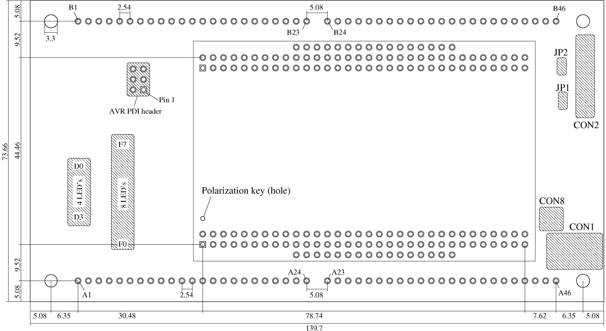
Click on the image for a larger version or download the PDF version.
Programming of the ATxmega and Examples
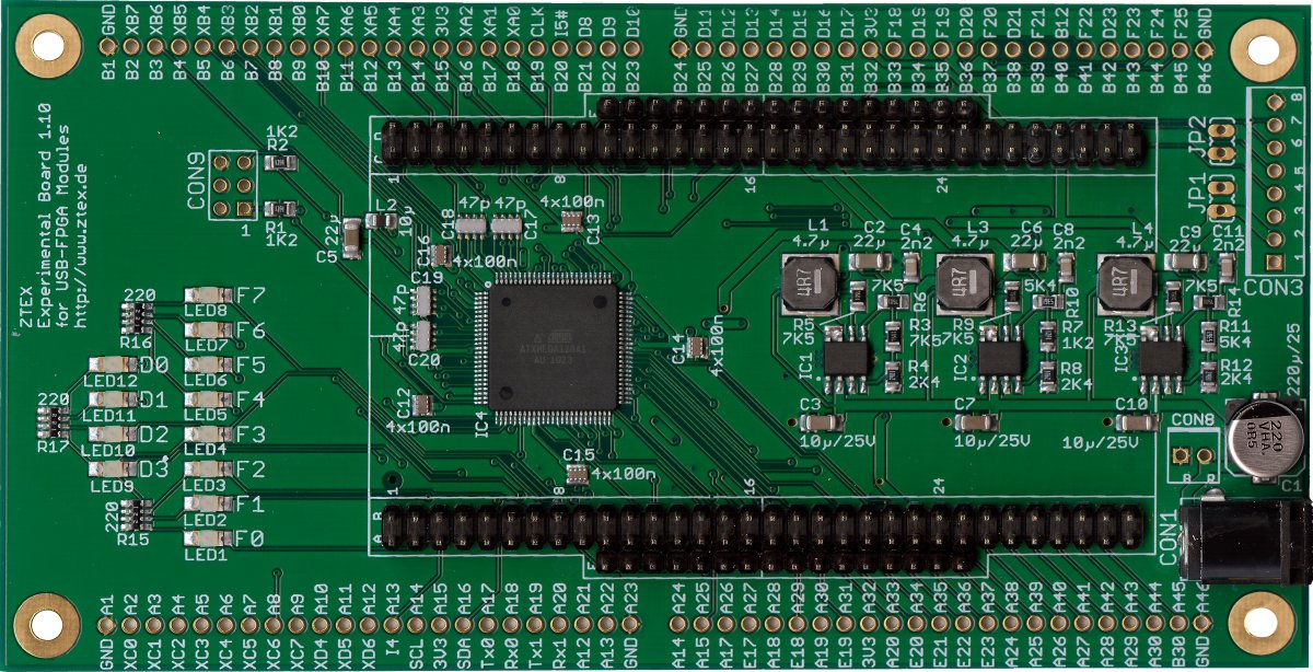
The ATxmega microcontroller can be programmed by the EZ-USB FX2 microcontroller via USB using the EZ-USB FX2 SDK or via AVR PDI header using the AVRISP mkII cable. The EZ-USB FX2 SDK also contains examples for the ATxmega and allows to access the non volatile memories (NVM).External power: CON1 and CON8
CON1 is a standard DC power jack with 2.1mm center pin diameter for a supply voltage of 4.5 V to 16 V.Alternatively CON8 can be used to connect non standard power cables. The ground pin of CON8 (quadratic pad) is marked with "B" and the supply pin (oval pad) is marked with "R", see the images below.
JTAG connector: CON3, JP1 and JP2
The pin description of the JTAG connector CON3 reads as follows:
| Pin | Description |
| 1 | +3.3V |
| 2 | +2.6V |
| 3 | Not connected |
| 4 | TMS |
| 5 | TCK |
| 6 | TDI |
| 7 | TDO |
| 8 | GND |
The voltage for the I/O signals (TCK,TMS,TDI,TDO) is 2.6V. Pin 2 can be used as supply for these signals. Pin 1 (+3.3V) can be used as supply for the JTAG adapter.
On USB-FPGA Modules 1.2 jumpers JP1 and JP2 can be closed to enforce JTAG configuration mode. But usually this is not required since the JTAG interface is always enabled. On USB-FPGA Modules 1.11 these jumpers have no function.
An appropriate power connector set for CON3 is delivered with the Experimental Board.
AVR PDI header
CON 9 is a standard AVR PDI header which can be used to program the ATxmega microcontroller using the AVRISP mkII programmer. The pin assignment reads as follows:| 6 GND |
5 CLK |
| 4 N/C |
3 N/C |
| 2 3.3V |
1 DATA |
LED's
All 12 LED's are connected to the ATxmega microcontroller. Eight of them (labelled F0 to F7) are connected to Port F and four of them (labelled D0 to D3) are connected to bits 0 to 3 of Port D.Analog Experimental Board I/O Connector
Four 1x23 pin connectors deliver I/O signals and voltages to user circuits.
The drawing shows the position of the connectors.
The Pinlist and the List of Connections are can be downloaded in Gnumeric or Excel format. The following table is is a short version the these files:
| Experimental Board 1.10 | USB-FPGA Boards | |||||||||
| I/O connector pin |
FX2 pin |
Spartan 3 USB-FPGA Module 1.2 FPGA pin |
Spartan 6 USB-FPGA Module 1.11 FPGA pin |
|||||||
| Pin | Pin name | XMEGA Pin |
LED | |||||||
| A1 | GND | |||||||||
| A2 | XC0 | PC0 | ||||||||
| A3 | XC1 | PC1 | ||||||||
| A4 | XC2 | PC2 | ||||||||
| A5 | XC3 | PC3 | ||||||||
| A6 | XC4 | PC4 | ||||||||
| A7 | XC5 | PC5 | ||||||||
| A8 | XC6 | PC6 | ||||||||
| A9 | XC7 | PC7 | ||||||||
| A10 | XD4 | PD4 | ||||||||
| A11 | XD5 | PD5 | ||||||||
| A12 | XD6 | PD6 | ||||||||
| A13 | I4 | A3 | 22 | |||||||
| A14 | SCL | A6 | 29 | |||||||
| A15 | 3.3V | |||||||||
| A16 | SDA | B6 | 30 | |||||||
| A17 | Tx0 | A8 | 40 | |||||||
| A18 | Rx0 | B8 | 41 | |||||||
| A19 | Tx1 | A9 | B15 | |||||||
| A20 | Rx1 | B9 | B16 | |||||||
| A21 | A12 | A12 | 74 | A14 | ||||||
| A22 | A13 | A13 | 76 | C13 | ||||||
| A23 | GND | |||||||||
| A24 | A14 | A14 | 78 | D12 | ||||||
| A25 | A15 | A15 | 80 | E11 | ||||||
| A26 | A17 | A17 | 83 | C10 | ||||||
| A27 | E17 | E17 | A10 | |||||||
| A28 | A18 | A18 | 85 | B12 | ||||||
| A29 | E18 | E18 | F9 | |||||||
| A30 | A19 | A19 | 87 | A9 | ||||||
| A31 | E19 | E19 | D9 | |||||||
| A32 | 3.3V | |||||||||
| A33 | A20 | A20 | 90 | C8 | ||||||
| A34 | E20 | E20 | A8 | |||||||
| A35 | E21 | E21 | B8 | |||||||
| A36 | E22 | E22 | E8 | |||||||
| A37 | E23 | E23 | E7 | |||||||
| A38 | A24 | A24 | 93 | A7 | ||||||
| A39 | A25 | A25 | 96 | E6 | ||||||
| A40 | A26 | A26 | 98 | C6 | ||||||
| A41 | A27 | A27 | 100 | A6 | ||||||
| A42 | A28 | A28 | 103 | C5 | ||||||
| A43 | A29 | A29 | 105 | A5 | ||||||
| A44 | A30 | A30 | 108 | A4 | ||||||
| A45 | B30 | B30 | 107 | C4 | ||||||
| A46 | GND | |||||||||
| B1 | GND | |||||||||
| B2 | XB7 | PB7 | ||||||||
| B3 | XB6 | PB6 | ||||||||
| B4 | XB5 | PB5 | ||||||||
| B5 | XB4 | PB4 | ||||||||
| B6 | XB3 | PB3 | ||||||||
| B7 | XB2 | PB2 | ||||||||
| B8 | XB1 | PB1 | ||||||||
| B9 | XB0 | PB0 | ||||||||
| B10 | XA7 | PA7 | ||||||||
| B11 | XA6 | PA6 | ||||||||
| B12 | XA5 | PA5 | ||||||||
| B13 | XA4 | PA4 | ||||||||
| B14 | XA3 | PA3 | ||||||||
| B15 | 3.3V | |||||||||
| B16 | XA2 | PA2 | ||||||||
| B17 | XA1 | PA1 | ||||||||
| B18 | XA0 | PA0 | ||||||||
| B19 | CLK | C3 | 52 | R16 | ||||||
| B20 | I5# | C5 | 84 | |||||||
| B21 | D8 | D8 | 5 | K16 | ||||||
| B22 | D9 | D9 | 4 | L16 | ||||||
| B23 | D10 | D10 | 2 | M16 | ||||||
| B24 | GND | |||||||||
| B25 | D11 | D11 | 1 | P16 | ||||||
| B26 | D12 | D12 | 141 | P15 | ||||||
| B27 | D13 | D13 | 140 | T15 | ||||||
| B28 | D14 | D14 | 137 | K15 | ||||||
| B29 | D15 | D15 | 135 | R14 | ||||||
| B30 | D16 | D16 | 132 | M13 | ||||||
| B31 | D17 | D17 | 131 | M12 | ||||||
| B32 | 3.3V | |||||||||
| B33 | F18 | F18 | M11 | |||||||
| B34 | D19 | D19 | 130 | T12 | ||||||
| B35 | F19 | F19 | M10 | |||||||
| B36 | D20 | D20 | 129 | R9 | ||||||
| B37 | F20 | F20 | T9 | |||||||
| B38 | D21 | D21 | 127 | N9 | ||||||
| B39 | F21 | F21 | P9 | |||||||
| B40 | B12 | B12 | 73 | B14 | ||||||
| B41 | F22 | F22 | T8 | |||||||
| B42 | D23 | D23 | 122 | P7 | ||||||
| B43 | F23 | F23 | R7 | |||||||
| B44 | F24 | F24 | T6 | |||||||
| B45 | F25 | F25 | T4 | |||||||
| B46 | GND | |||||||||
| XD7 | PD7 | D22 | 124 | N8 | ||||||
| XE0 | PE0 | E13 | A13 | |||||||
| XE1 | PE1 | E14 | C11 | |||||||
| XE2 | PE2 | E15 | A11 | |||||||
| XE3 | PE3 | E16 | B10 | |||||||
| XE4 | PE4 | B14 | 77 | D11 | ||||||
| XE5 | PE5 | B15 | 79 | F10 | ||||||
| XE6 | PE6 | B18 | 84 | A12 | ||||||
| XE7 | PE7 | B17 | 82 | E10 | ||||||
| XH0 | PH0 | B19 | 86 | C9 | ||||||
| XH1 | PH1 | B20 | 89 | D8 | ||||||
| XH2 | PH2 | B24 | 92 | C7 | ||||||
| XH3 | PH3 | B25 | 95 | F7 | ||||||
| XH4 | PH4 | B26 | 97 | D6 | ||||||
| XH5 | PH5 | B27 | 99 | B6 | ||||||
| XH6 | PH6 | B28 | 102 | D5 | ||||||
| XH7 | PH7 | B29 | 104 | B5 | ||||||
| XR1 | PR1 | C9 | 93 | |||||||
| XR0 | PR0 | C10 | 92 | |||||||
| PDI/RESET | RESET/PDI | C11 | 91 | |||||||
| PDI | PDI | C12 | 90 | |||||||
| XQ3 | PQ3 | C13 | 89 | |||||||
| XQ2 | PQ2 | C14 | 88 | |||||||
| XQ1 | PQ1 | C15 | 87 | |||||||
| XQ0 | PQ0 | C16 | 86 | |||||||
| PJ7 | PJ7 | C20 | 128 | P8 | ||||||
| PJ6 | PJ6 | C21 | 125 | M9 | ||||||
| PJ5 | PJ5 | C22 | 123 | T7 | ||||||
| PJ4 | PJ4 | C23 | 119 | M7 | ||||||
| PJ3 | PJ3 | C24 | 116 | N6 | ||||||
| PJ2 | PJ2 | D24 | 118 | P6 | ||||||
| PJ1 | PJ1 | C25 | 112 | M6 | ||||||
| PJ0 | PJ0 | D25 | 113 | P4 | ||||||
| XK7 | PK7 | F10 | N16 | |||||||
| XK6 | PK6 | F11 | M15 | |||||||
| XK5 | PK5 | F12 | R15 | |||||||
| XK4 | PK4 | F13 | L14 | |||||||
| XK3 | PK3 | F14 | N14 | |||||||
| XK2 | PK2 | F15 | L13 | |||||||
| XK1 | PK1 | F16 | L12 | |||||||
| XK0 | PK0 | F17 | R12 | |||||||
| PF0 | LED1 | |||||||||
| PF1 | LED2 | |||||||||
| PF2 | LED3 | |||||||||
| PF3 | LED4 | |||||||||
| PF4 | LED5 | |||||||||
| PF5 | LED6 | |||||||||
| PF6 | LED7 | |||||||||
| PF7 | LED8 | |||||||||
| PD3 | LED9 | |||||||||
| PD2 | LED10 | |||||||||
| PD1 | LED11 | |||||||||
| PD0 | LED12 | |||||||||
Images
Click on the images for larger versions.
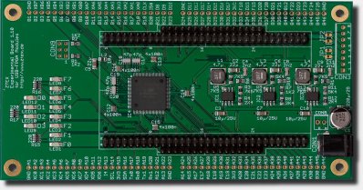
Analog Experimental Board 1.10. |
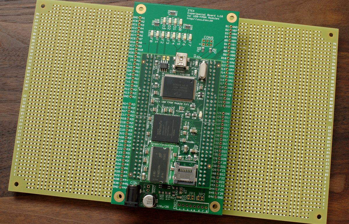
Analog Experimental Board with Spartan 6 USB-FPGA Module 1.11 and two Expansion Boards.
|
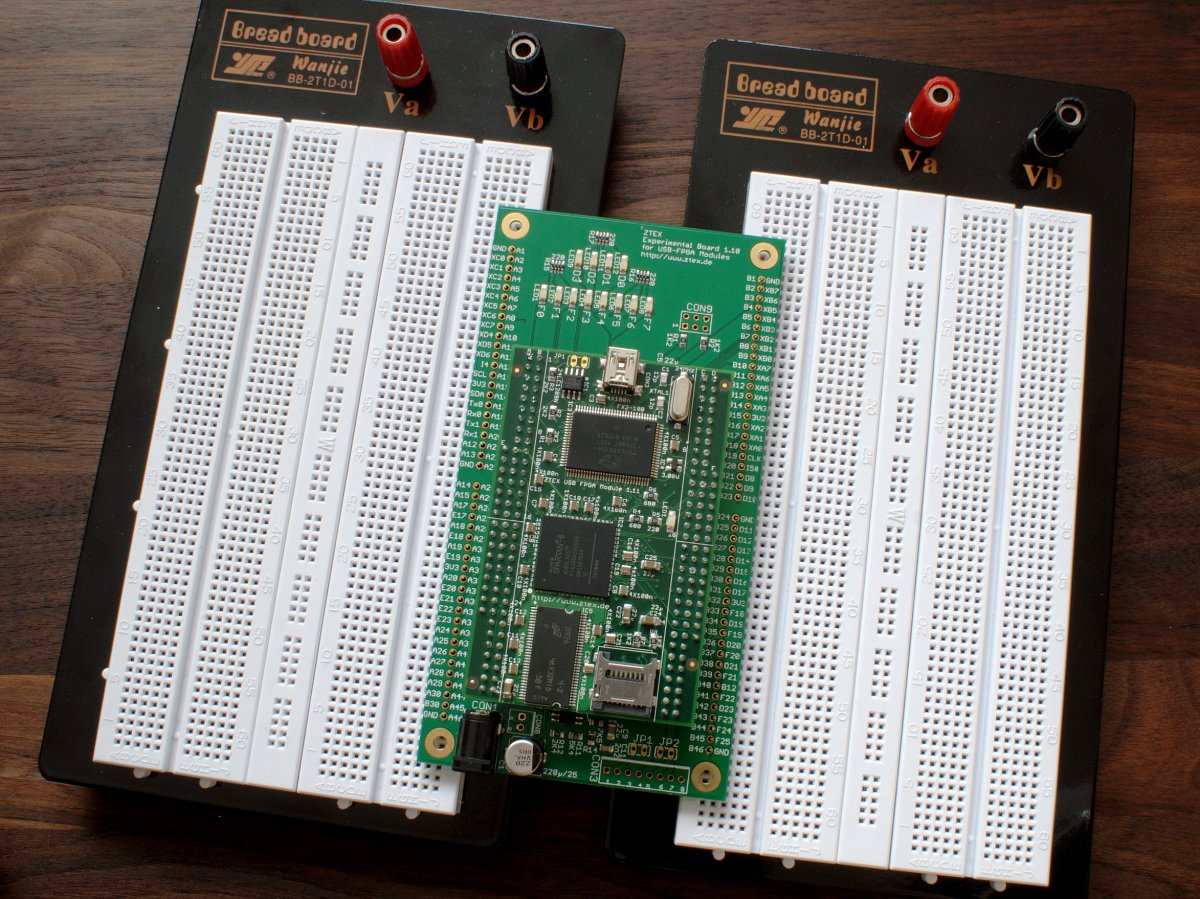
Analog Experimental Board with Spartan 6 USB-FPGA Module 1.11 and two Breadboards.
|