USB-FPGA Module 2.04:
Spartan 6 FPGA Board with EZ-USB FX2 and DDR SDRAM
USB-FPGA Modules 2.04 have been discontinued due to market situation (more than 5 years lead time for the Spartan 6 FPGA's). Please switch to USB-FPGA Modules 2.13.
|
Block diagram
Schematics (PDF) |
 |
Block diagram
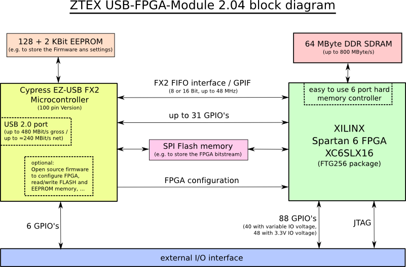
Features
- USB 2.0 interface with Mini-USB connector (B-type)
- Cypress CY7C68013A EZ-USB FX2 Microcontroller (100 pin version)
- Xilinx Spartan 6 XC6SLX16 FPGA (XC6SLX9 and XC6SLX25 on request)
- External I/O connector (consisting in two female 2x32 pin headers with 2.54mm grid) provides:
- 88 General Purpose I/O's (GPIO) connected to FPGA
- 6 General Purpose I/O's (GPIO) connected to EZ-USB FX2 Controller
- 6 Special I/O's (SIO) connected to EZ-USB FX2 Controller
- JTAG signals
- Reset signal
- External power (4.5 V .. 16 V) input
- 3.3V output
- I/O voltage output or input, see External I/O connector
-
64 MByte DDR SDRAM:
- 200 MHz clock frequency
- 16 Bit bus width
- Up to 800 MByte/s data rate
- Easy to use hard memory controller included Spartan 6 FPGA with 6 ports. (see SDK for examples)
- 128 MBit on-board Flash memory
- Allows Bitstream loading from Flash to FPGA (up to 6.5 MByte/s)
- Accessible from EZ-USB FX2 and from FPGA
- 128 Kbit EEPROM memory (can be used to store the EZ-USB firmware)
- 2 Kbit MAC-EEPROM: contains a unique non erasable MAC-address and is used to store firmware settings
- On-Board power supply:
- 3.3 V: 2000 mA
- 2.5 V: 2000 mA
- 1.2 V; 1000 mA
- Temperature range: 0-70°C
Variants
| Variant | FPGA | Speed grade (larger means faster) |
Availability |
| USB-FPGA Module 2.04a | XC6SLX9 | 2C | Not available |
| USB-FPGA Module 2.04b | XC6SLX16 | 2C | Sold out. Will not produced anymore due to market situation (lead time of the FPGA is more than 5 years). |
| USB-FPGA Module 2.04c | XC6SLX25 | 2C | Not available |
All variants are supported by the free ISE Webpack versions.
Functional description
The following drawing shows the measurements and the location of the components described here.
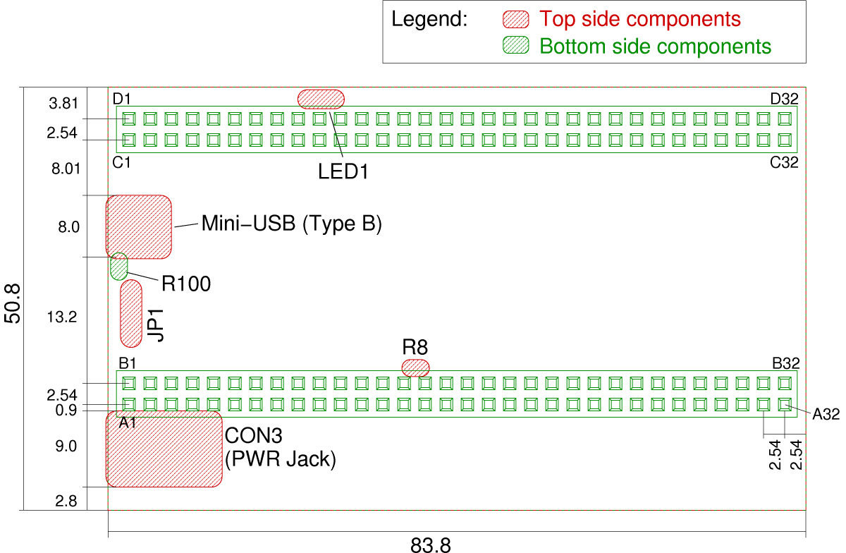
Click on the image for a larger version or download the PDF version.
USB-FPGA Modules 2.04 have no mounting holes because they are usually plugged onto an application circuit. Alternatively also one of the add-on cards may be used as mounting adapter.
Common functions of all Series 2 FPGA Boards
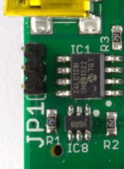
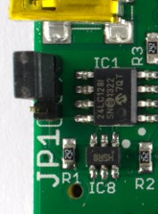
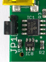
USB-FPGA Modules 2.04 belong to ZTEX FPGA Board Series 2. All functions that are shared with the other members of this Series are described on the Series 2 FPGA Board pageEEPROM address: JP1
Jumper JP1 specifies the I2C address of the EEPROM:
| JP1 | I2C address |
| open | 0xA2 |
| close | 0xAA |
JP1 is used tp prevent Firmware booting from EEPROM, e.g. if the firmware is corrupt. At booting the EZ-USB FX2 Microcontroller expects the firmware at the I2C address 0xA2 (jumper open) and falls back to an internal firmware if no valid data is found at this address (jumper closed).
JP1 has an unconnected pin which can be used for parking the jumper. The following pictures show all possible jumper positions:
|
|
| JP1 open | JP1 closed |
FPGA state: LED1
LED1 indicates the configuration state of the FPGA as follows:
| LED1 | FPGA |
| on | unconfigured |
| off | configured |
Power connector: CON3
External power can be supplied via CON3 or pins A1 and B1 of the external I/O connector. CON3 is a standard DC power jack with 2.1mm center pin (+) diameter and 5.5mm barrel (-) diameter. Valid supply voltage is 6 V to 16 V. A1 and B1 of the I/O connector and the center pin of CON3 are connected directly. This allows to supply a base board from the FPGA board.For applications that use the memory at full speed USB standard does not guaranty sufficient current in order to power USB-FPGA Modules 2.04. Nevertheless, the FPGA Board can be powered from USB if the optional 0 Ω resistor R100 (package 0805) is installed (bottom side below USB connector, see drawing). In that case care must be taken in order to prevent that no second power external power supply is connected to CON3 or pins A1 and B1 of the external I/O connector.
Clock resources
On the FPGA board two clocks sources are connected to the FPGA: the clock output of the EZ-USB FX2 which is usually configured to 48 MHz and the interface clock which can be configured to 30 MHz or to 48 MHz. They can be used to generate new clocks within the FPGA using DCM's or PLL's.Additional clocks can be connect to the GCLK pins of the I/O connector.
In most cases the on board clock sources are sufficient.
Flash
USB-FPGA Modules 2.04 have 128 MBit SPI Flash memory which can be accessed by the EZ-USB FX2 microcontroller and the FPGA and may serve as configuration memory for the FPGA.The maximum configuration speed is 6.5 Mbyte/s and is achieved at 26 MHz SPI Bus speed and 2 Bit SPI Bus width (bitgen settings -g ConfigRate:26 -g SPI_buswidth:2). Bitstream can be written to the Flash by the SDK via USB (most comfortable) or via JTAG using the indirect programming method of the Xilinx Tools, see ZTEX Wiki
If Flash is not used (CS signal high) the other three SPI pins (DIN, CLK and DOUT) can be used as GPIO pins.
I/O Connector
The external I/O connector is compatible to other FPGA Boards of the Series 2 and therefore described at page of Series 2 FPGA Boards.On USB-FPGA Modules 2.04 only 88 (of 100) pins from the I/O connector are assigned to FPGA. The remaining 12 pins are connected to Port E (6 pins) and to SIO signals (6 pins) of the EZ-USB FX2 microcontroller.
40 FPGA GPIO pins at rows A and B have the variable I/O voltage VCCO_AB, I/O voltage of remaining pins is fixed to 3.3V. By default VCCO_AB is connected to 3.3V through the 0Ω resistor R8 and is therefore a 3.3V output. (This is the standard behaviour for all FPGA Boards of the Series 2.) If another I/O voltage is required, R8 has to be unsoldered and VCCO_AB is used as voltage input. (The VCCO_CD pins of the I/O connector are permanently connected to 3.3V.)
Further details can be found in the Pin assignment table in Gnumeric and Excel format.
JTAG
The FPGA can be configured either via USB or via JTAG. JTAG signals are available on the external I/O connector and JTAG headers are installed on most add-on cards.
Images
Click on the images for larger versions.
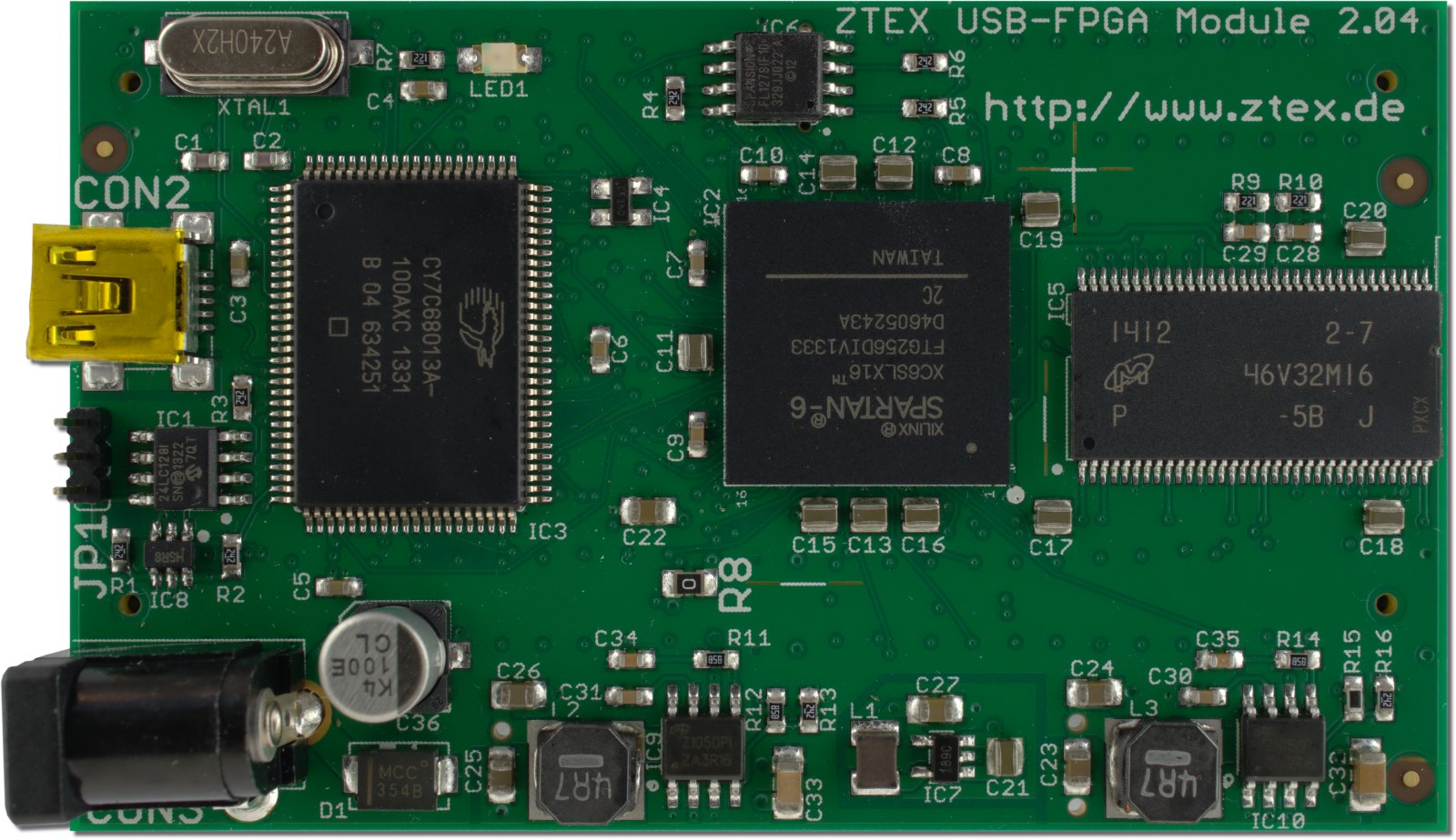
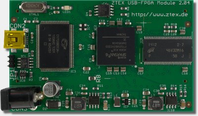
Top side of USB-FPGA Module 2.04b with Spartan 6 XC6SLX16. |
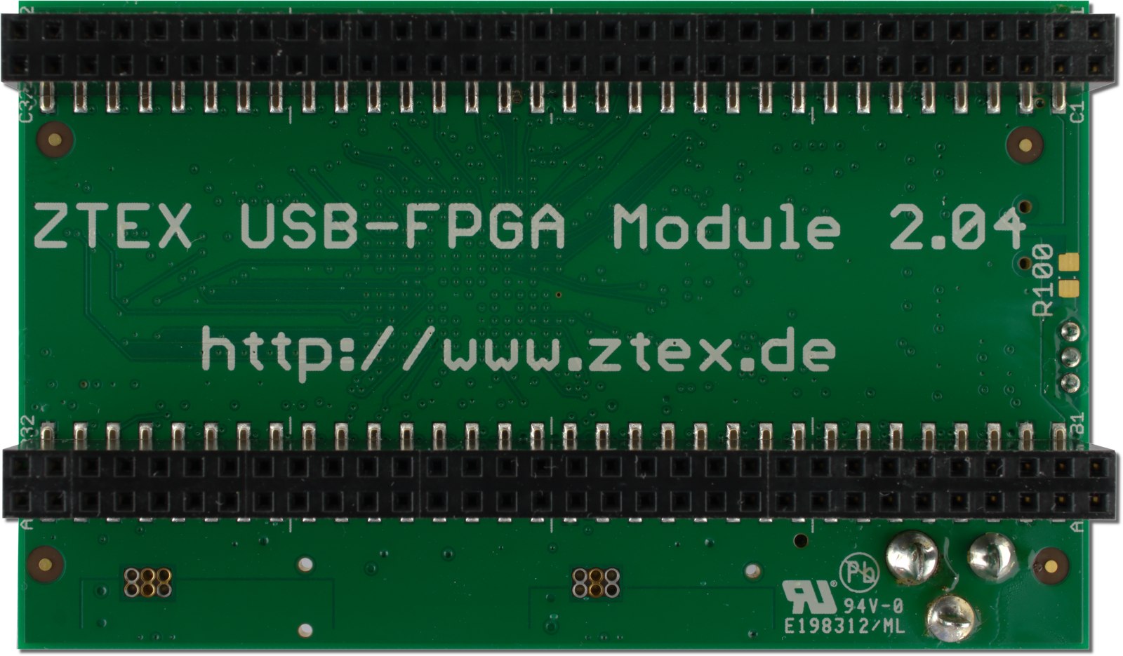
Bottom side of USB-FPGA Module 2.04. |