|
|
ZTEX FPGA Boards with Open Source SDK
ZTEX develops and sells FPGA Boards. Our products are mainly designed for prototyping and small series development but may also be used as
evaluation or development kit.
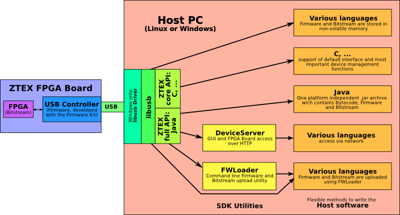
A powerful Open Source SDK is available for our products.
By using a firmware with Default Interface in combination with a Device Server it is even possible
to access our FPGA board without development of special software.
|
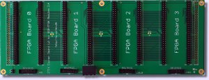
FPGA Boards
|
|---|
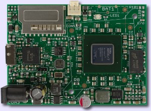
USB-FPGA Module 2.18
• FPGA Board with Xilinx Artix 7 XC7A200T,
• USB 3.0 using EZ-USB FX3,
• 100 GPIO's (General Purpose I/O's),
• 256 MB DDR3 SDRAM,
• On-board power supply and Flash memory.
|
|
USB-FPGA Module 2.16
• FPGA Board with Xilinx Artix 7 XC7A200T,
• 100 GPIO's (General Purpose I/O's),
• On-board power supply and Flash memory,
• USB 2.0 interface (using EZ-USB FX2).
|
|
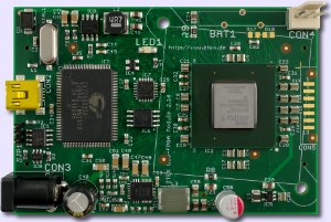
USB-FPGA Module 2.14
• FPGA Board with Xilinx Artix 7 XC7A15T to XC7A100T,
• USB 3.0 using EZ-USB FX3,
• 100 GPIO's (General Purpose I/O's),
• 256 MB DDR3 SDRAM,
• On-board power supply and Flash memory.
|
|
|
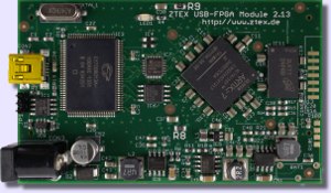
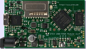
USB-FPGA Module 2.13
• FPGA Board with Xilinx Artix 7 XC7A35T to XC7A100T,
• 100 GPIO's (General Purpose I/O's),
• 256 MB DDR3 SDRAM,
• On-board power supply and Flash memory,
• USB 2.0 interface (using EZ-USB FX2).
|
|
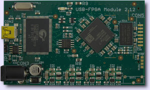
USB-FPGA Module 2.12
• FPGA Board with Xilinx Artix 7 XC7A15T to XC7A50T,
• 100 GPIO's (General Purpose I/O's),
• 256 MB DDR3 SDRAM,
• On-board power supply and Flash memory,
• USB 2.0 interface (using EZ-USB FX2).
|
|
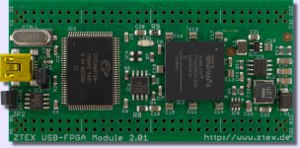
USB-FPGA Module 2.01
• FPGA Board with Xilinx Spartan 6 LX16,
• 100 GPIO's (General Purpose I/O's),
• On-board power supply and Flash memory,
• USB 2.0 interface (using EZ-USB FX2).
|
|
|
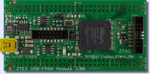
FPGA Module 2.00
• FPGA Board with Xilinx Spartan 6 LX16,
• 100 GPIO's (General Purpose I/O's),
• On-board power supply and dual Flash memory,
• On-Board JTAG and SPI header.
|
|
|
|
ZTEX SDK
|
|---|
The Open Source SDK allows rapid development of platform-independent host software using a Default Firmware
with standardized interface. Custom firmware for EZ-USB FX2 and FX3 controllers can be created using the Firmware Kit.
|
|
Add-On Cards for FPGA Boards
|
|---|
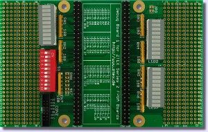
Debug Board
30 LED's, 4 switches and JTAG header for debugging
and prototyping with Series 2 FPGA Boards.
|
|
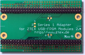
Series 1 Adapter
Adapts Series 2 FPGA Boards to application circuits for Series 1.
|
|
|
|
|
|